SOLAR CELL DIMENSIONS
Four cell shapes are permitted. Their dimensions are defined in the figure below. See the
wafer calculator for more information on cell shapes.

TYPES OF GRID ELEMENTS
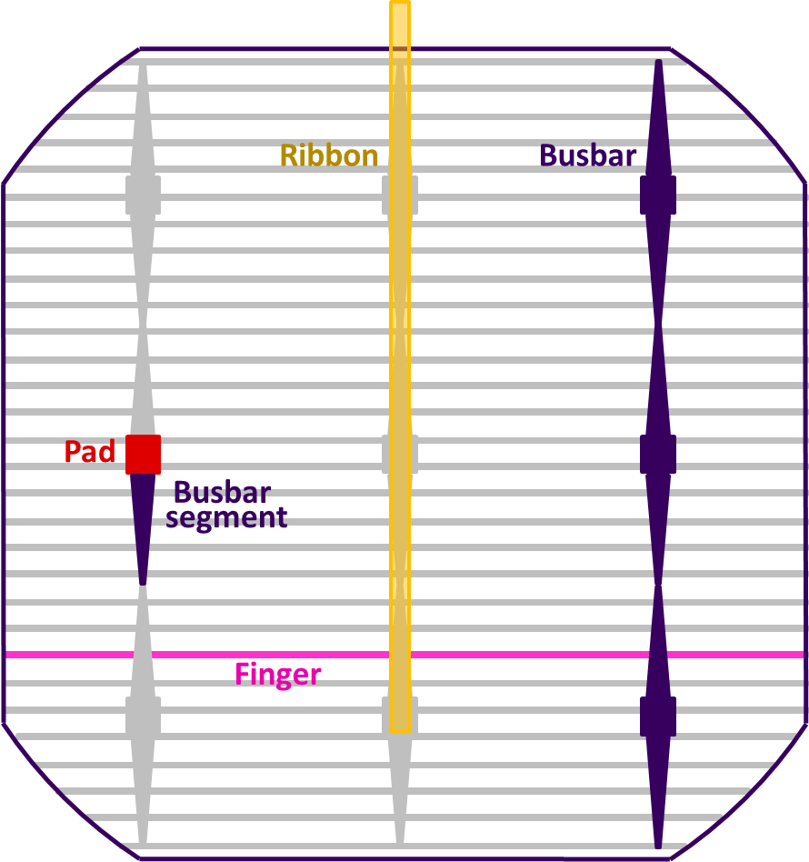
There are four types of grid elements: fingers, busbars, pads and ribbons. One of each is highlighted
in the figure below. This figure gives an example of the many grid designs that can be simulated with the grid calculator.
In the example, the cell's shape is pseudosquare. Its metal grid consists of 30 fingers and three busbars, where each busbar is comprised of
three pads and six busbar segments. In the example, the fingers have a constant width and the busbar segments are tapered, but it is also
possible to simulate fingers that are tapered and busbars that have a constant width.
When ribbons are included, they overlap the busbars and make contact to the busbars' pads. The example shows just one of the three
ribbons so that the underlying elements can be seen.

OPTIONS FOR THE SOLAR CELL DEISGN
All of the solar cells simulated in this calculator have two metal contacts: an N-type contact and a P-type contact.
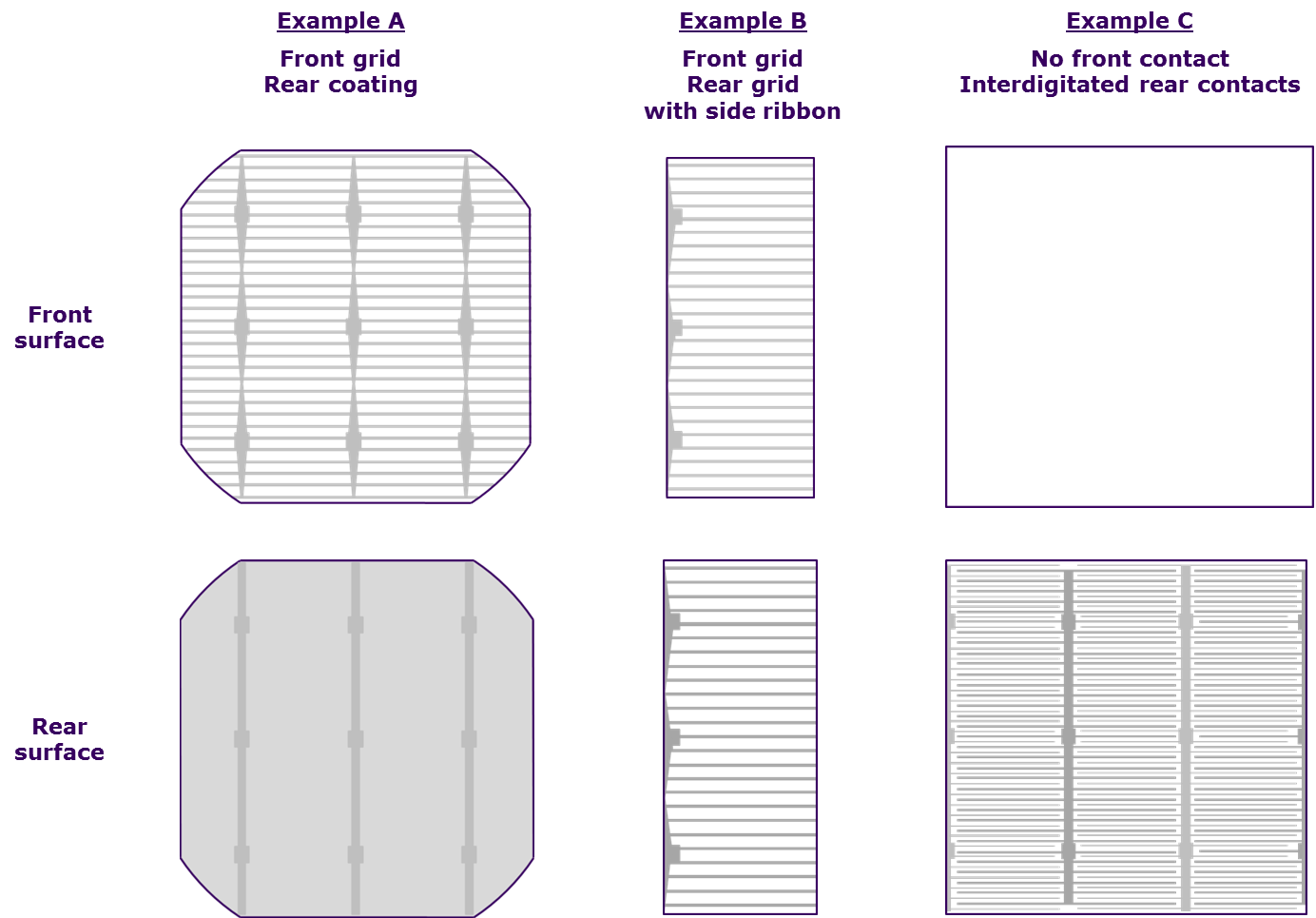
Three examples of how the contacts can be laid out are illustrated below.
In Examples A and B, one contact is on the front and the other is on the rear. These are usually
called "front-contact solar cells". In Example C, both contacts are on the rear and they form an interdigitated grid.
These cells are usually called "interdigitated back-contact" (IBC) or "all-back-contact" (ABC) solar cells.
The grid calculator gives the option of selecting an "N-type grid", a "P-type grid" or "no contacts" for the front.
This third option is only available to square and rectangular wafers.
When a grid contact is chosen for the front, the contact on the rear must be of the opposite type. It can be either a
full metal coating like Example A, or a metal grid like Example B. Thus, if one selects an N-type grid for the front, the rear
can have a P-type coating or a P-type grid.
When the front has no contacts, the rear must contain interdigitated contacts like Example C.
Finally, for a cell with a front metal grid and a single busbars, it is possible to
place that busbar on the side or in the centre of the wafer. Example B shows the layout of a rectangular solar cell with a front
and rear grid where the busbar is on the side of the solar cell. In the current version of the grid calculator, a busbar can
only be placed on the side of square and rectangular solar cells.

CROSS SECTIONS OF THE GRID ELEMENTS
Four cross-sectional profiles are permitted for the grid elements. Their dimensions are defined in the figure below. The
fourth cross section, labelled "PseudoRectangular", is handy but not commonly used. It is defined as two semicircles and a rectangle,
and has two variants: (a) wide, when W > 2H, and (b) narrow, when W < 2H. It is semicircular when W = 2H.

TAPERING OF THE GRID ELEMENTS
The fingers and busbars can have a constant width or they can be tapered. The figure below illustrates these options for an element
with a rectangular cross section. In the current version of the grid calculator, the pads and ribbons are only permitted to have a constant width.
When a finger is tapered, its minimum and maximum width are defined.
In cases where the fingers have different lengths—such as when the cell has curved edges or the busbars are tapered—then
the minimum and maximum widths are assigned to the longest finger. The tapering gradient of this longest finger is determined
from the equation (Wmax – Wmin) / L, and that gradient is applied to all
fingers on the cell. The fingers then all have
the same Wmin and the same tapering gradient, which means that shorter fingers have a smaller
Wmax.
The procedure for assigning dimensions to tapered busbars is the same as for tapered fingers. That is, all busbar segments have the same
minimum width and tapering gradient, where the tapering gradient is determined from the longest busbar segment.

DIMENSIONS OF THE GRID ELEMENTS
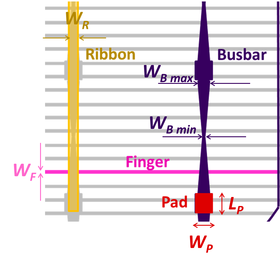
The user defines a height H and a width W to each element type. When an element is tapered, its width is defined with
a minimum Wmin and maximum Wmax as described above. The user also defines the length of the pad
LP, whereas the length of every other element is calculated from the cell shape, the contact design, and the number of elements.
The widths for a single grid pattern are defined in the figure below. In this example, the fingers are not
tapered; if they were, it would be necessary to define their minimum and maximum widths. And in this example, the busbars are tapered,
although they don't need to be.

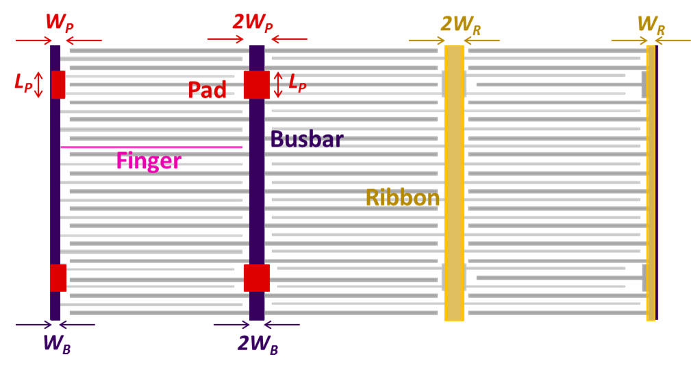
The widths of interdigitated grid elements are slightly more complicated. When there are three or more ribbons, then at
least one ribbon is located centrally rather than at the side. These central ribbons, and the underlying pads and busbars, receive current
from fingers on both sides, whereas the side ribbons receive current from fingers on just one side. Consequently, the central elements must be
twice as wide as the side elements (excepting the fingers, of course), as illustrated in the figure below.
In the grid calculator, the widths defined for an interdigitated grid are assigned to the side elements. If there are any central ribbons,
pads or busbars, these are taken to be twice as wide.

In all of these designs, it is possible to assign different widths for P and N contacts (except for the ribbons). Keep in mind, therefore,
that the widths of ribbons, pads and busbars for an interdigitated cell are defined as if the element were on the side of the cell.
The width for central elements will be twice as wide as the input widths.
OUTPUTS
Five outputs are listed:
| |
|
| Rs: |
The series resistance of the solar cell. |
| Shading: |
The percentage of the front surface that is shaded by metal. This percentage does not consider the light that reflects from the metal onto the solar cell. |
| A: |
The surface area of the solar cell that is covered with metal. Note that since ribbons lie on top of the pads, busbars and fingers, the total surface area
on a surface can be less than the sum of its constituents. |
| V: |
The volume of metal on the solar cell. |
| Cost: |
The cost of the metal on the solar cell. |