Quokka Manual
1. Overview
Quokka is a free software tool specialized for the fast simulation of silicon solar cell devices in one to three dimensions. It employs simplifications to the general semiconductor carrier transport model, which results in much less computational effort compared to alternative simulation software. Those simplifications, namely quasi-neutrality and conductive boundaries, are well validated to not impose notable loss of generality or accuracy for wafer-based silicon solar cell devices. Thus Quokka enables to simulate even moderately complex 3D silicon solar cell device geometries in short computation times on standard computers, while providing a similar level of accuracy and generality as state-of-the-art commercial device simulation software.
The main modelling difference to most other device simulation software comes with the conductive boundary simplification. Here near-surface regions, for example an emitter diffusion, are not modelled in detail by defining the doping profile and surface recombination etc. The inputs required are rather lumped properties of such regions, most importantly the sheet resistance and the effective recombination characteristic like for example the emitter saturation current density J0e. This is well suitable if those inputs are the ones derived e.g. experimentally, but makes Quokka not (directly) applicable if for example an optimization of the doping profile is of interest.
Quokka essentially solves for the steady-state electrical characteristics of the device, and is capable to derive various typical solar cell characteristics: fixed terminal voltage, fixed terminal current, open-circuit (OC) conditions, maximum-power-point (MPP) conditions, short-circuit-current (Jsc) conditions, light- and dark-IV curve, quantum-efficiency (QE) curve, suns-Voc curve and series-resistance (Rs) curve. A notable extension is the inclusion of luminescence modelling, which allows Quokka to simulate for example spatially and spectrally resolved photo-luminescence characteristics.
While being powerful enough to simulate many silicon solar cell designs and conditions of practical interest, Quokka’s scope is to be highly accessible for both newcomers and simulation experts. This is realized by the meshing and the solver numerics being largely automated and by using a pre-defined but flexible geometry layout, so that the required user inputs are reduced to a minimum and specifically designed for typical silicon solar cell conditions. Furthermore, Quokka automatically finds typical cell conditions of interest like maximum power point, and features an optimizer routine to fit unknown device properties to output characteristics. The software is hosted on pvlihgthouse.com.au, where Quokka can be downloaded for free and support resources as well as a web-based settings file generator can be found.
Although these measures enable to perform extensive simulation tasks with little knowledge about fundamentals of numerical simulation, it is reminded that Quokka still is a full multidimensional solver with a large space of possible input combinations. As with any such complex tool the principle of “garbage in, garbage out” is still highly applicable, and limits of solvable conditions exist. In particular users intending to produce sensitive simulation results, for example for scientific publications, are strongly encouraged to follow the considerations in Computational Performance and Accuracy.
2. INSTALLING AND RUNNING QUOKKA
2.1 INSTALLATION
Quokka is a compiled MATLAB program and requires the Matlab Comiler Runtime (MCR) 2013b to be installed. The MCR is freely available from the Mathworks website, be sure to download the correct (NOT the latest) version, 2013b:
The latest Quokka version is available for download as Windows 32bit / 64bit, Linux and OSX version:
The zip archive contains the Quokka executable as well as some example settings and input data files.
2.2 SETTINGS FILE AND PVL SETTINGS FILE GENERATOR
All settings required to define the simulation setup are given in the settings file. This is a Matlab script file (.m), which is however in ascii format and can therefore be modified with any text editor. While it is possible to directly edit the settings file, it is recommended to use the settings file generator on PVLighthouse, a web-based GUI which creates the settings file in a more user-friendly and less error-prone way:
Note that any input data files required for the simulation must be in the same directory as the settings file. Also all solution data will be stored in this directory.
2.3 RUNNING A SIMULATION
2.3.1 GUI
The easiest way to run the simulation is using the little GUI, which opens by default when starting Quokka.
Figure 1: Quokka GUI
Table 1: Description of GUI Elements
| GUI Element | Description and comments |
|---|---|
| Select different settings file |
Browse and select one or multiple settings files.
No reload is required when the settings file is modified. |
| Display Geometry |
This is good practice to do before running the simulation as a quick sanity check for the geometry definition and resulting number of elements
For multiple settings files only the first one will be displayed Sweep and optimizer settings are ignored In the Figure which opens up (see Figure 2) one can rotate and zoom, and toggle the visibility of selected features: xyz axis, F front side, R rear side, M metal coverage and S symmetry sides For multiple conductive boundaries of the same type a higher sheet resistance will be of lighter colour than the lower one, which can be useful for validating the arrangement of the respective boundaries The latter must not be mistaken with shaded colours, which indicates a contacted region |
| Start Simulation |
Starts the simulation, plots and saves results if finished successfully
Multiple settings files will be run sequentially |
| Abort |
Aborts the simulation at selected points
Only limited functionality for parallel simulations |
| Overwrite results files | When checked, Quokka will not append date and time to the result files |
| Sweep: save spatial data | When checked, Quokka will save all spatial data for each parameter during a sweep |
| Messages | Displays status and error messages |
Figure 2: Geometry display figure
2.3.2 Command line options
When starting the Quokka executable from the command prompt, additional messages are displayed, and some additional functionality can be enabled by command line options, see Table 2.
For example, to run settings1.m and settings2.m parallelized on 5 CPUs in Windows:
- Quokka2.exe cores5 settings1.m settings2.m
Starting those settings file in Linux as a background job without graphical output and redirecting command line output to nohup.out:
- nohup ./Quokka2 cores5 no_display settings1.m settings2.m > nohup.out &
Table 2: Description of command line options
| Command line option | Description and comments |
|---|---|
| *.m |
Settings file to be simulated, *.m must be replaced by an actual unique filename
Multiple settings files can be assigned and will be simulated sequentially; this saves the overhead to startup Quokka for each simulation |
| sweep_store_spatial_data | Quokka will save all spatial data for each parameter during a sweep |
| coresX |
Enables parallel simulation mode, where X needs to be replaced by the desired number of parallel threads (max. 12 in Matlab 2013b)
Only QE-curves, non-automatic IV-curves, sweeps and sequential optimization are executed in parallel, and the parallel mode will consequently not increase the speed of other simulations Limited messaging and abort functionality |
| no_display | Prevents the GUI and any graphic figures to open |
| overwrite_results | Quokka will not append date and time to the result files |
| sweep_store_spatial_data | Quokka will save all spatial data for each parameter during a sweep |
3. Settings
3.1 Basic concept
The input parameters are organized in several groups, which is loosely also reflected in the PVL settings file generator. These comprise geom (overall solution domain and contact geometry), bulk (bulk properties), bound (boundary conditions, i.e. diffusion and surface properties), generation (optics / generation), circuit (external circuit), lumi (luminescence modelling), sweep (parameter sweep) and optim (iterative optimization / curve fitting).
A standout input parameter is circuit.terminal, which controls at what operating point(s) the device will be simulated, and consequently what output characteristic is achieved. There is a qualitative difference between single operating point conditions, like a fixed terminal voltage, and “curves” consisting of many different operating conditions, like an IV-curve.
The sweep functionality sits “on top” and must be distinguished from the “curve” circuit.terminal options. If a curve terminal option is set together with a parameter sweep, the respective curve will be simulated for each sweep parameter.
The optimizer sits further “on top” on the sweep functionality, and the sweep can therefore not be used to run multiple optimizations with different input parameters. Such a “sequential optimization” must rather be defined using vector assignments to the optim.override inputs. The sweep can be used to create x-y value pairs for curve fitting. However, most common targets are readily produced by the curve terminal options, for example an IV curve by “IV_curve” and effective lifetime curve by “sunsVoc_curve”.
3.2 Description of input parameters
Table 3: Full list of input parameters, green and orange highlights parameters applicable only to FRC or IBC version, respectively; where applicable, default settings applied when no input is given are marked with an *
| Parameter name | Units | Typical value range | Description | Applicability / dependencies |
|---|---|---|---|---|
| Geometry | ||||
| version.design | ‘FRC’ ‘IBC’ | pre-defined geometry layout to use, see Predefined Layouts. | ||
| geom.dimensions | 1, 2 or 3 | 1D, 2D or 3D simulation | ||
| geom.Wz | µm | 50 … 500 | device thickness (z-direction) | |
| geom.Wx | µm | 1 … 10000 | unit cell width in x-direction | 2D and 3D only |
| geom.Wxfront | µm | 1 … 10000 | front unit cell width in x-direction | if different, values must be integer and must have a reasonably low lcm, see Predefined Layouts. |
| geom.Wxrear | µm | 1 … 10000 | rear unit cell width in x-direction | |
| geom.Wy | µm | 1 … 10000 | unit cell width in y-direction | 3D only |
| geom.frontcont.shape | ‘circle’ ‘rectangle’ ‘line’ ‘full’ | shape of front (emitter) contact(s) in 2D, ‘circle’, ‘rectangle’ and ‘line’ produce identical geometry in 3D, ‘line’ will be orientated in y-direction | 2D and 3D only | |
| geom.rearcont.shape | ‘circle’ ‘rectangle’ ‘line’ ‘full’ | shape of rear contact(s) in 2D, ‘circle’, ‘rectangle’ and ‘line’ produce identical geometry in 3D, ‘line’ will be orientated depending on the defined contact position, see Predefined Layouts. | 2D and 3D only | |
| geom.frontcont.wx | µm | 1 … 10000 | half-width of front contact(s) in x-direction radius for ‘circle’ | 2D and 3D only |
| geom.frontcont.wy | µm | 1 … 10000 | half-width of front contact(s) in y-direction | 3D only only for ‘rectangle’ contact shape |
| geom.rearcont.wx | µm | 1 … 10000 | half-width of rear contact(s) radius for ‘circle’ | 2D and 3D only |
| geom.rearcont.wy | µm | 1 … 10000 | half-width of front contact(s) in y-direction | 3D only only for ‘rectangle’ contact shape |
| geom.rearcont.position | [1] … [1 3] … [1 2 3 4] | vector with any combination of positions 1 to 4; defines the corner(s) where a rear contact exists, see Predefined Layouts; all contacts have same shape and dimensions. | 2D and 3D only positions 3 and 4 in 3D only | |
| geom.leftcont.shape | ‘circle’ ‘rectangle’ ‘line’ | shape of left (emitter) contact(s) in 2D, ‘circle’, ‘rectangle’ and ‘line’ produce identical geometry in 3D, ‘line’ will be orientated in y-direction | ||
| geom.rightcont.shape | ‘circle’ ‘rectangle’ ‘line’ | shape of right contact(s) in 2D, ‘circle’, ‘rectangle’ and ‘line’ produce identical geometry in 3D, ‘line’ will be orientated depending on the defined contact position, see Predefined Layouts. | ||
| geom.lefttcont.wx | µm | 1 … 10000 | half-width of left contact(s) in x-direction radius for ‘circle’ | |
| geom.leftcont.wy | µm | 1 … 10000 | half-width of left contact(s) in y-direction | 3D only only for ‘rectangle’ contact shape |
| geom.rightcont.wx | µm | 1 … 10000 | half-width of right contact(s) radius for ‘circle’ | 2D and 3D only |
| geom.rightcont.wy | µm | 1 … 10000 | half-width of right contact(s) in y-direction | 3D only only for ‘rectangle’ contact shape |
| geom.leftcont.numberx | 0.5, 1, 1.5 … | multiple of 0.5 defining the number of “half” left (emitter) contacts in x-direction within the unit cell, see Predefined Layouts. | ||
| geom.leftcont.pitchx | µm | 1 … 1000 | full pitch of multiple left (emitter) contacts within the unit cell | only for numberx > 0.5 |
| geom.rightcont.numberx | 0.5, 1, 1.5 … | multiple of 0.5 defining the number of “half”right contacts in x-direction within the unit cell, see Predefined Layouts. | ||
| geom.rightcont.pitchx | µm | 1 … 1000 | full pitch of multiple right contacts within the unit cell | only for numberx > 0.5 |
| geom.leftcont.w_metal | µm | 0 … 10000 | left (emitter) metal half width, influences optics only | |
| geom.rightcont.w_metal | µm | 0 … 10000 | right metal half width, influences optics only | |
| geom.leftcont.y_position | ‘aligned’ ‘opposite’ ‘double’ ‘half’ | position of left (emitter) contact(s) relative to right contact(s) in y-direction, see Predefined Layouts. | 3D only | |
| geom.meshquality | 1,2,3 or ‘user’ | 1: coarse (sufficient for most simulations), 2: medium, 3: fine, ‘user’: use expert settings below | ||
| geom.dzminfront | µm | 0.2 … 2 | element size in z-direction at the front surface | for ‘user’ mesh quality only |
| geom.dzminfront | µm | 0.2 … 2 | element size in z-direction at the rear surface | for ‘user’ mesh quality only |
| geom.dxmin | µm | 0.2 … 20 | minimum element size in x-direction | 2D and 3D only for ‘user’ mesh quality only |
| geom.dymin | µm | 0.2 … 20 | minimum element size in y-direction | 3D only for ‘user’ mesh quality only |
| geom.dxmax | µm | 1 … 500 | maximum element size in x-direction | 2D and 3D only for ‘user’ mesh quality only |
| geom.dymax | µm | 1 … 500 | maximum element size in y-direction | 3D only for ‘user’ mesh quality only |
| geom.scale | 3 … 20 | determines minimum element sizes in x- and y-direction via dividing the smallest respective features (contact dimensions, gap etc.) by this number | 2D and 3D only for ‘user’ mesh quality only | |
| geom.inflation | 1 … 5 | maximum allowable ratio of neighbouring element sizes; effectively controls how fast mesh sizes are increased away from feature edges | for ‘user’ mesh quality only | |
|
Bulk properties
Note that all recombination mechanisms are always active and additive, see Quokka Physics |
||||
| bulk.type | ‘p-type’ ‘n-type’ | doping type | ||
| bulk.rho | Ohm.cm | 0.1 … 1000 | bulk resistivity | |
| bulk.T | K | 300K* | temperature; carefully check validity of applied models and inputs if changing temperature | |
| bulk.nk | ‘Green08_Nguyen14’* ‘Green08_300K’ | silicon optical properties, used for 1D_model generation and luminescence modeling | ||
| bulk.mobility | ‘Klaassen’* ‘Arora’ 'Fixed' | mobility model, see Quokka Physics | ||
|
bulk.mun bulk.mup |
cm²/Vs | constant electron / hole mobility | ‘fixed’ mobility only | |
| bulk.nieff | ‘default’* ‘fixed’ | ‘default’: see Quokka Physics ‘fixed’: user value | ||
| bulk.nieffvalue | cm-3 | ~1e10 | fixed value of nieff | for ‘fixed’ bulk.nieff only |
| bulk.taub | µs | 1 … 1e5 | fixed “background” bulk lifetime set to very high value (e.g. 1e10) to disable | |
| bulk.Auger | ‘Richter2012’* ‘Altermatt2011’ ‘Kerr2002’ ‘Sinton1987’ ‘off’ | Auger recombination model, see Quokka Physics | ||
| bulk.Brad | cm3/s | 4.73e-15* | radiative recombination coefficient set to 0 to disable radiative recombination | |
| bulk.SRH.BO.Nt | cm-3 | 0* … 1e18 | oxygen concentration for BO-complex recombination, see Quokka Physics. delete or set to zero to disable | for p-type bulk only |
| bulk.SRH.BO.m | 2 … 4 | processing dependent parameter for BO-complex recombination | for p-type bulk only | |
| bulk.SRH.midgap.taun0 | µs | 1 … 1e5 | fundamental electron lifetime for midgap (defect level = Fermi level) SRH recombination | |
| bulk.SRH.midgap.taup0 | µs | 1 … 1e5 | fundamental hole lifetime for midgap (defect level = Fermi level) SRH recombination | |
| bulk.SRH.custom{i}.Nt | cm-3 | defect density of i-th SRH defect | ||
| bulk.SRH.custom{i}.Et_Ei | eV | -0.5 … 0.5 | defect level of i-th SRH defect, relative to intrinsic energy | |
| bulk.SRH.custom{i}.sigman | cm² | electron capture cross section of i-th SRH defect | ||
| bulk.SRH.custom{i}.sigmap | cm² | hole capture cross section of i-th SRH defect | ||
|
boundary conditions
Index {i} stands for the i-th conductive- / nonconductive boundary condition, see Defining Multiple Boundary Regions. Each boundary can have a contacted and a non-contacted region with different recombination properties assigned to .cont. and .noncont, respectively The IBC version does not support contacted non-conductive boundaries |
||||
| bound.conduct{i}.location | ‘front’ ‘rear’ ‘left’ ‘right’ | location of the i-th conductive boundary front and left located conductive boundaries are the “emitter” for FRC and IBC version, respectively | ||
| bound.nonconducti{i}.location | ‘front’ ‘rear’ | location of non-conductive boundary | ||
| bound.conduct{i}.cont.rec bound.nonconduct{i}.cont.rec bound.conduct{i}.noncont.rec bound.nonconduct{i}.noncont.rec | ‘J0’ ‘S’ ‘expr’ | How to model boundary recombination; by constant saturation current density J0, constant effective surface recombination velocity S or analytical expression | ||
| bound.conduct{i}.cont.J0 bound.nonconduct{i}.cont.J0 bound.conduct{i}.noncont.J0 bound.nonconduct{i}.noncont.J0 | A/cm² | 0 … 1e-10 | saturation current density note the unit is A/cm², NOT fA/cm² | only for ‘J0’ recombination model |
| bound.conduct{i}.cont.S bound.nonconduct{i}.cont.S bound.conduct{i}.noncont.S bound.nonconduct{i}.noncont.S | cm/s | 0 … 1e6 | effective surface recombination velocity 1e6 represents “infinite” recombination limited by carrier transport to the boundary; higher values therefore do not make any difference other than potentially causing numerical problems | only for ‘S’ recombination model |
| bound.conduct{i}.cont.expr bound.nonconduct{i}.cont.expr bound.conduct{i}.noncont.expr bound.nonconduct{i}.noncont.expr | A/cm² | ‘expression’ |
analytical expression resulting in a boundary recombination current in A/cm²
Variables allowed to be used:
dn
: excess carrier density at the boundary in cm-3
const.N
: bulk doping density in cm-3
const.nieff
: bulk intrinsic carrier density in cm-3
const.n0
: equilibrium minority carrier density in cm-3
const.T
: temperature in K
const.Vt
: thermal voltage in V
const.q
: elementary charge in As
e.g.: ‘10*dn*const.q‘
(corresponds to Seff = 10 cm/s) |
only for ‘expr’ recombination model |
| bound.conduct{i}.cont.J02 bound.nonconduct{i}.cont.J02 bound.conduct{i}.noncont.J02 bound.nonconduct{i}.noncont.J02 | A/cm² | 0* … 1e-6 | n=2 saturation current density | only for ‘J0’ recombination model |
| bound.conduct{i}.type | ‘p-type‘ ‘n-type‘ | conduction type of front conductive boundary in IBC version | ||
| bound.conduct{i}.Rsheet | Ω | 1 … 10000 | Sheet resistance | |
| bound.conduct{i}.shape | ‘full‘ ‘line‘ ‘rectangle‘ ‘circle‘ ‘contact‘ | shape of conductive boundary is always aligned to any contact(s) of the same type ‘contact’ sets the shape identical to the same type contact defined in the geometry group | 2D and 3D only not applicable for IBC front conductive boundary (always full area) | |
| bound.conduct{i}.wx | µm | 1 … 10000 | width of conductive boundary in x-direction; radius for ‘circle’ | 2D and 3D only |
| bound.conduct{i}.wy | µm | 1 … 10000 | width of conductive boundary in y-direction | 3D only ‘rectangle’ shape only |
| bound.conduct{i}.jctdepth | µm | 0* … 10 | junction depth | |
| bound.conduct{i}.colleff | ‘fixed’ ‘ext_file’ | how to model collection efficiency, see Quokka Physics | junction depth >0 | |
| bound.conduct{i}.colleff_value | 0 … 1* | fixed value for collection efficiency | ‘fixed’ collection efficiency only | |
| bound.conduct{i}.colleff_filename | ‘filename’ | load collection efficiency from external file, see External File Format | ‘ext_file’ collection efficiency only | |
| generation | ||||
| generation.type | ‘1D_model’ ‘Jgen_surface’ ‘Jgen_uniform’ ‘ext_file’ ‘customdata’ ‘off’ | how to derive generation profile ‘1D_model’: models generation profile by optical properties, see Quokka Physics ‘Jgen_surface’, ‘Jgen_uniform’: applies user-defined generation current to the illuminated surface or uniformly distributed through the device thickness | ||
| generation.Jgen | mA/cm² | ~40 | user defined total generation current | ‘Jgen_surface’, ‘Jgen_uniform’ generation or with Jgen_correction=1 |
| generation.Jgen_correction | 0* 1 | 1: scales the external or ‘1D_model’ generation profile to match a desired total generation current defined by generation.Jgen | ‘1D_model’, ‘ext_file’ and ‘customdata’ generation only | |
| generation.ext_file | ‘filename’ | load generation profile from external file, see External File Format | ‘ext_file’ generation only | |
| generation.customdata | µm cm-3s-1 | [z1, z2, … zn; G1, G2, … Gn] | generation profile with n value pairs; z: distance to illuminated surface G: generation rate | ‘customdata’ generation only |
| generation.spectrum | ‘AM1.5g‘ ‘monochromatic‘ ‘custom‘ | defines the illumination spectrum | ‘1D_model’ generation only | |
| generation.monochromatic.wavelength | nm | 250 … 1450 | monochromatic illumination wavelength | ‘monochromatic’ spectrum only |
| generation.monochromatic.flux | cm-2s-1 | ~2e17 | photon flux of monochromatic illumination | ‘monochromatic’ spectrum only |
| generation.facet_angle | ° | 0 or 54.7 | facet angle of illuminated surface texture; set to 0 for planar surface | ‘1D_model’ generation only |
| generation.spectrum_custom | nm Wm-2nm-1 | [λ1, λ2, … λn; I1, I2, … In] | custom spectrum with n value pairs: λ: wavelength I: spectral intensity | ‘custom’ spectrum only |
| generation.transmission | ‘fixed’ ‘ext_file’ ‘custom’ | how (wavelength dependent) transmission at the illuminated surface is defined ‘fixed’: fixed value for all wavelengths | ‘1D_model’ generation only | |
| generation.transmission_value | 0 … 1 | fixed value for front transmission | ‘fixed’ transmission only | |
| generation.transmission_filename | ‘filename’ | load front transmission data from external file, see External File Format | ‘ext_file’ transmission only | |
| generation.transmission_custom | nm | [λ1, λ2, … λn; T1, T2, … Tn] | transmission curve with n value pairs: λ: wavelength T: transmission | ‘custom’ transmission only |
| generation.Z | ‘fixed‘ ‘ext_file‘ ‘custom‘ ‘param‘ ‘limit_4n2‘ ‘limit_Green02‘ | how (wavelength dependent) pathlength enhancement is defined | ‘1D_model’ generation only | |
| generation.Z_value | 0 … 1 | fixed value for pathlength enhancement | ‘fixed’ Z only | |
| generation.Z_filename | ‘filename’ | load pathlength enhancement data from external file, see External File Format | ‘ext_file’ Z only | |
| generation.Z_custom | nm | [λ1, λ2, … λn; Z1, Z2, … Zn] | pathlength enhancement curve with n value pairs: λ: wavelength Z: pathlength enhancement | ‘custom’ Z only |
| generation.Z0 | 1 … 1000 | Z0 for Z-parameterization | ‘param’ Z only | |
| generation.Zinf | 1 … 3 | Zinf for Z-parameterization | ‘param’ Z only | |
| generation.Zp | 1 … 10 | Zp for Z-parameterization | ‘param’ Z only | |
| generation.suns | 0 ... 1 ... 10 | scales the generation (AND intensity for efficiency calculation) | ||
| generation.illum_side | ‘front’ ‘rear’ | defines the illuminated side of the device | ||
| generation.shading_width | µm | 0 … 10000 | half shading width by metal fingers, independent of the contact width; Is applied as a line shading in y-direction centred to each contact on the illuminated side | 2D and 3D only |
| generation.profile_type | ‘standard’ ‘cumulative’ | ‘cumulative’ expects PC1D-type profile | ‘ext_file’ and ‘customdata’ only | |
| external circuit | ||||
| circuit.terminal | ‘Vuc’ ‘Vterm’ ‘Jterm’ ‘OC’ ‘MPP’ ‘Jsc’ ‘light_IV_auto’ ‘IV_curve’ ‘QE_curve’ ‘sunsVoc_curve’ ‘Rs_curve’ | what “terminal” condition to solve single operating point conditions: ‘Vuc’: fixed unit cell voltage (fastest because no iterations required) ‘Vterm’: fixed terminal voltage ‘Jterm’: fixed terminal current ‘OC’: open-circuit (do NOT set high series / contact resistance as in PC1D) ‘MPP’: maximum power point ‘Jsc’: short-circuit-current (NOT short-circuit, voltage will be >0, but extracted current will be Jsc) “curve” terminal condition: ‘light_IV_auto’: automated algorithm to quickly but accurately derive light IV-curve and parameters (Voc, Jsc, FF, eta) ‘IV_curve’: solve at multiple user defined voltages ‘QE_curve’: quantum efficiency at multiple user defined wavelengths ‘sunsVoc_curve’: solve at multiple user defined suns-values ‘Rs_curve’: extract voltage dependent series resistance via double-light method; solves two automated light-IV curves with slightly different generation; advice: set circuit.IV_accuracy to at least 5 for smooth and accurate results | ||
| circuit.Vuc.value | V | 0.3 … 1 | unit cell voltage (BEFORE external circuit elements); avoid values close to zero, see Short-circuit Limitations | ‘Vuc’ terminal only |
| circuit.Vterm.value | V | 0.3 … 1 | terminal voltage (AFTER external circuit elements); avoid values close to zero, see Short-circuit Limitations | ‘Vterm’ terminal only |
| circuit.Jterm.value | mA/cm² | -40 … 1000 | terminal current | ‘Jterm’ terminal only |
| circuit.IV.mode | ‘Vterm’ ‘Vuc’ | whether to define unit cell (faster) or terminal voltages (slower) for IV_curve solution | ‘IV_curve’ terminal only | |
| circuit.IV.V_values | V | [V1, V2, … Vn] | n voltage values for IV_curve | ‘IV_curve’ terminal only |
| circuit.IV.init_previous | 0* 1 | 1: use solution from previous results as starting guess; faster and more stable for closely spaced IV points; disables parallel simulation of IV-curve 0: initialize start values for each IV point; more robust for largely spaced IV points | ‘IV_curve’ terminal only | |
| circuit.QE.wavelength_values | nm | [λ1, λ2, … λn] | n wavelength values for QE_curve | ‘QE_curve’ terminal only |
| circuit.sunsVoc.suns_values | [s1, s2, … sn] | n suns values for sunsVoc_curve | ‘sunsVoc_curve’ terminal only | |
| circuit.DJ0 | A/cm² | 0*… 1e-7 | saturation current density of external diode, see Quokka Physics | requires circuit.Dn |
| circuit.Dn | 1 … 4 | ideality factor of external diode, see Quokka Physics | required if circuit.DJ0 is defined | |
| circuit.Voc_guess | V | 0.67* | guess of Voc for iteration starting point; better guess can speed up the simulation | ‘OC’, ‘MPP’ and ‘light_IV_auto’ terminal only |
| circuit.IV_accuracy | 1* … 10 | higher value increases the number of points simulated on the light IV-curve does NOT influence the accuracy of IV-curve parameters (Voc, Jsc, FF, eta) >= 5 is recommended for ‘Rs_curve’ terminal option | ‘light_IV_auto’ and ‘Rs_curve’ terminal only | |
|
luminescence modelling
For luminescence modelling “front” always refers to the detection side which could actually be the rear side |
||||
| lumi.enable | 1 0 | switch luminescence on (1) or off (0) if off, no further inputs are required | ||
| lumi.scale | a.u. | simply scales the simulated luminescence signal can be used to convert simulated detected photon flux into measurement units, e.g. counts/s | ||
| lumi.normalize_signal | 1 0 | whether to normalize (1) the simulated signal or not (0); will normalize the spectrum and / or intensity map to its respective peak value | ||
| lumi.detection_side | ‘illuminated’ ‘opposite’ | whether the sensor detects luminescence from the illuminated or non-illuminated side | ||
| lumi.filter | ‘none’ ‘ext_file’ | how to define wavelength dependent transmission from the sample surface to the sensor (i.e. lens and filter transmission) ‘none’: 100% transmission | ||
| lumi.filter_filename | ‘filename’ | load optics transmission data from external file, see External File Format | ‘ext_file’ filter only | |
| lumi.sensor_EQE | ‘unity’ ‘silicon’ ‘ext_file’ | how to define wavelength dependent external quantum efficiency of sensor ‘unity’: 100% EQE ‘silicon’: calculates EQE assuming Lambert-Beer-Law for absorption with silicon absorption coefficient and sensor thickness | ||
| lumi.sensor_thickness | µm | thickness of sensor for calculation of EQE; more correctly, this is the total pathlength which is directly inserted into the Lamber-Beer-Law | ‘silicon’ sensor EQE only | |
| lumi.sensor_EQE_filename | ‘filename’ | load sensor EQE from external file, see External File Format | ‘ext_file’ sensor EQE only | |
| lumi.wavelength_start | nm | 800* … 1400 | lower bound of wavelength to include into modeling | |
| lumi.wavelength_end | nm | 800 … 1400* | upper bound of wavelength to include into modeling | |
| lumi.emission_function | 1 2 3 4 | how to model internal optics, see Quokka Physics 1: both sides planar, quasi-1D 2: both sides textured, quasi-1D 3: general, quasi-1D; further inputs required, see below; set of default values approximately applicable for typical textured front and semi-planar rear solar cell devices 4: both sides lambertian, 2D and 3D geometrical blurring; user-defined mesh settings with relatively low dxmax (and dymax) recommended for smooth and accurate results; can be highly computationally intensive | 4: 2D and 3D only | |
| lumi.internal_refl | ‘default’ ‘ext_file’ | how to define wavelength dependent internal surface reflectivity ‘default’: assumes planar silicon – air interface on both sides | not applicable for emission function 2 | |
| lumi.internal_refl_filename | ‘filename’ | load internal reflectivity for front and rear surface from external file, see External File Format | ‘ext_file’ internal reflectivity only | |
| lumi.general.facet_angle | ° | 0 … 54.7 | facet angle of front surface texture set to zero for planar surface | emission function 3 only |
| lumi.general.lambertian_factor | 0 … 1 | lambertian factor of rear side 0: completely specular 1: completely diffuse | emission function 3 only | |
| lumi.general.refRear | 0 … 0.6* … 1 | internal rear reflectivity | emission function 3 only | |
| lumi.general.refFrontS | 0 … 0.62* … 1 | first internal front reflectivity | emission function 3 only | |
| lumi.general.refFrontN | 0 … 0.93* … 1 | n-th internal front reflectivity | emission function 3 only | |
| lumi.geometrical.number_reflections | 0 … 20 | number of internal reflections to trace high number might add significant computational effort | emission function 4 only | |
|
parameter sweep
Index {i} stands for the i-th dependent sweep parameter All dependent sweep parameters must have the same number of values To have only one independent (group of) sweep parameter(s), assign values only to one (group) (…_1 or …_2) |
||||
| sweep.enable | 1 0 | switch parameter sweep on (1) or off (0) if off, no further inputs are required | ||
| sweep.param_1{i} sweep.param_2{i} | ‘input parameter‘ | input parameter to sweep within the first / second independent group of sweep parameters, e.g.: ‘bulk.rho‘ must exactly match an input parameter existing within the settings file | ||
| sweep.values_1{i} sweep.values_2{i} | same as i-th sweep parameter | [v1, v2, … vn] {‘S1‘, ‘S2‘, … ‘Sn‘} |
sweep values for i-th sweep parameter of the first / second independent group of sweep parameters
can be numeric (v) or strings (S)
sweeping of some string values including external file names NOT possible yet
to disable the second (group of) independent sweep parameter(s):
sweep.value_2{1}=[]; |
|
|
optimizer
Index {i} stands for the i-th parameter to optimize / the i-th goal to achieve / the i-th override rule to apply For sequential optimization, each vector input must have the same length n |
||||
| optim.enable | 2 1 0 | switch off / change mode of optimizer 2: curve fitting mode 1: goal mode 0: off; not further input required | ||
| optim.maxiter | 5 … 50 | maximum number of iterations; aborts once this number is reached | ||
| optim.accuracy | 0.1 … 1* … 10 | influence termination tolerances higher values potentially increases accuracy but at the cost of increased number of iterations and increased likelihood of “stuck” optimizations | ||
| optim.param{i} | ‘input parameter‘ | input parameter to optimize, e.g.: ‘bulk.rho‘ must exactly match an input parameter existing within the settings file | ||
| optim.start{i} | same as i-th optim. parameter | same as i-th optim. parameter | start value of parameter to optimize should be carefully chosen not far from the final result for good convergence | |
| optim.lb{i} | same as i-th optim. parameter | same as i-th optim. parameter | lower bound of allowed values for parameter to optimize <optim.start{i} | |
| optim.ub{i} | same as i-th optim. parameter | same as i-th optim. parameter | upper bound of allowed values for parameter to optimize >optim.start{i} | |
| optim.goal{i} | ‘scalar result‘ e.g. ‘results.eta’ | name of i-th goal to achieve; must be a scalar within the results structure produced by the simulation setup, see Table 5 | mode 1 only | |
| optim.value{i} | same as scalar result defined in i-th goal | ‘max’ ‘min’ v [v1, v2, … vn] | value of i-th goal to achieve; ‘max’: maximises the result ‘min’: minimises the result v: (vector of) numerical value(s) | mode 1 only ‘min’ and ‘max’ only for a single goal i=1 |
| optim.goalx |
‘vector result’
e.g.
‘results.curves
.navg’ |
name of x-values to achieve must be a vector within the results structure produced by the simulation setup, see Table 5 | mode 2 only | |
| optim.goaly |
‘vector result’
e.g.
‘results.curves
.taueff’ |
name of y-values to achieve must be a vector within the results structure produced by the simulation setup with the same length as the one defined in optim.goalx, see Table 5 | mode 2 only | |
| optim.xyfile | ‘filename’ | external file containing x-y-value pairs which define the target curve to fit to | mode 2 only | |
| optim.override.param{i} | ‘input parameter’ | name of i-th parameter to override during the optimization | ||
| optim.override.value{i} | ‘expression’ v [v1, v2, … vn] | override value to assign during the optimization ‘expression’: analytical expression containing the parameter(s) to optimize, e.g.: ‘bulk.rho*5’ v: (vector of) numerical value(s) | ||
4. Data input / output
4.1 External file format
Several inputs like for example a generation profile can be defined via external files. Those files must be located in the same directory as the settings file and the containing data must be correctly organized to be usable by Quokka.
Accepted file formats are either Excel files (.xls or .xlsx) or ASCII files (.txt or .csv). Note that only “proper” Excel files can be read, while those produced with alternative tools, like for example by the PVLighthouse website, can cause reading errors. This can be fixed by opening and saving them in Excel. For the ASCII files, most common delimiters are supported. Furthermore, a comma decimal separator is supported, which takes slightly longer to import due to internal string replacement.
The data must be organized in columns, where the first two (three) columns contain the input data and the first row can optionally be a header row or the first data row. Table 4 summarizes the data organization for the different external file inputs.
Table 4: Data organization in external files
| Assigned to input parameter | First column | Second column | Third column |
|---|---|---|---|
| generation.ext_file | distance to illuminated surface in µm | generation rate in cm-3s-1 | |
| generation.transmission_filename | wavelength in nm | front transmission 0 … 1 | |
| generation.Z_filename | wavelength in nm | pathlength enhancement Z | |
| bound.conduct{i}.colleff_filename | wavelength in nm | collection efficiency 0 … 1 | |
| lumi.filter_filename | wavelength in nm | transmission 0 … 1 | |
| lumi.sensor_EQE_filename | wavelength in nm | EQE 0 … 1 | |
| lumi.internal_refl_filename | wavelength in nm | front reflectivity 0 … 1 | rear reflectivity 0 … 1 |
| optim.xyfile | same quantity and unit as defined in optim.goalx | same quantity and unit as defined in optim.goaly |
4.2 Data Output
Naturally, what output data is available depends on what characteristics the device is solved for. A basic distinction is between single operating point and multiple operating points characteristics. Only for a single operating point a unique electrical condition with unique spatial results, including luminescence results, is present and will be stored. This is not the case for the curve terminal conditions ‘IV_curve’, ‘sunsVoc_curve’ and ‘Rs_curve’, and consequently no spatial and luminescence output is available. Outstanding operating points exist for ‘light_IV_auto’ (maximum power point) and ‘QE_curve’ (short circuit current conditions) and therefore spatial data is available for those, as well as for all single operating point terminal conditions ‘Vuc’, ‘Vterm’, ‘Jterm’, ‘OC’, ‘MPP’ and ‘Jsc’.
When a sweep is performed, no spatial data will be available by default, however can be stored for each parameter by activating the corresponding switch, see Running A Simulation.
4.2.1 Graphical output
The kind of graphical output is predefined and dependent on what terminal condition was solved, and whether a sweep or optimization task was performed. Spatial data will only be plotted when a single point terminal condition was set, respective curves will be shown for curve terminal conditions, and the variation of few major scalar outputs for a parameter sweep. Beyond that, there is no influence by the user on the graphical output. All important results are stored in a csv and Matlab file, the latter containing also spatial output if applicable, from which users must create custom graphics themselves.
4.2.2 Results files
Quokka saves two results files, a .csv file containing most scalar and curve outputs, and a .mat file containing additional results including spatial output data (if available). The .mat file is a Matlab file format, which can be read by several software tools, but is naturally best processed in Matlab. If the optimizer is used, the results will be saved in files which include ‘optim’ in the file name (with some additional outputs not listed below).
Table 5: List of output quantities contained in the .csv and / or .mat results file; nomenclature according to .mat file, .csv file is equivalent
| Output quantity | Units | Description |
|---|---|---|
| Scalar outputs | ||
| Vterm | mV | terminal voltage (including external circuit elements) |
| Jterm | mA/cm² | terminal current density (including external circuit elements) |
| Vuc | mV | unit cell voltage (excluding external circuit elements) |
| Juc | mA/cm² | unit cell current density (excluding external circuit elements) |
| Voc | mV | open circuit voltage (@ 1 sun for suns-Voc curve) |
| Jsc | mA/cm² | short-circuit current density (total generation current density @ 1 sun for suns-Voc curve) |
| FF | % | fill factor of light-IV curve (pseudo fill factor for suns-Voc curve) |
| eta | % | efficiency (pseudo efficiency for suns-Voc curve) |
| Vmpp | mV | terminal voltage at maximum power point |
| Jmpp | mA/cm² | terminal current density at maximum power point |
| navg | cm-3 | average minority carrier density |
| taueff | µs | effective lifetime, definition see Quokka Physics |
| conduct | S | excess conductivity, definition see Quokka Physics |
| JL_two_diode | mA/cm² | current density source from two-diode model fit |
| J01_two_diode | A/cm² | ideal saturation current density from two-diode model fit |
| J02_two_diode | A/cm² | non-ideal (n=2) saturation current density from two-diode model fit |
| Rseries_two_diode | Ωcm² | series resistance from two-diode model fit |
| Rshunt_two_diode | Ωcm² | shunt resistance from two-diode model fit |
| Rseries_mpp_pow | Ωcm² | series resistance @ MPP from power loss, definition see Quokka Physics |
| Rseries_mpp_DLM | Ωcm² | series resistance @ MPP from double light method |
| lumi_mean | a.u. | average luminescence signal (detected photon flux times scaling factor) |
| computing_time | s | total computing time (not correct when optimizer is used) |
| JGbulk | mA/cm² | generation current density of the bulk |
| JGfront | mA/cm² | generation current density of the front conductive boundaries |
| JGfront | mA/cm² | generation current density of the rear conductive boundaries |
| N | cm-3 | bulk doping density |
| nieff | cm-3 | effective intrinsic carrier density |
| n0 | cm-3 | equilibrium minority carrier density |
| FELA outputs (see Quokka Physics for definitions) | ||
| FELA.gen | mW/cm² | generated power |
| FELA.res_bulk_n | mW/cm² | resistive loss from electron transport in the bulk |
| FELA.res_bulk_p | mW/cm² | resistive loss from hole transport in the bulk |
| FELA.res_front_conduct FELA.res_left_conduct | mW/cm² | resistive loss in the front / left conductive boundary(ies) |
| FELA.res_front_cont FELA.res_left_cont | mW/cm² | resistive loss from front / left contact resistance |
| FELA.res_rear_conduct FELA.res_right_conduct | mW/cm² | resistive loss in the rear / right conductive boundary(ies) |
| FELA.res_rear_cont FELA.res_right_cont | mW/cm² | resistive loss from rear / right contact resistance |
| FELA.res_front | mW/cm² | IBC only: resistive loss in the front conductive boundary |
| FELA.rec_Auger | mW/cm² | intrinsic bulk recombination loss (Auger and radiative) |
| FELA.rec_SRH | mW/cm² | other bulk recombination loss (SRH and fixed bulk lifetime contributions) |
| FELA.rec_front_conduct FELA.rec_left_conduct | mW/cm² | recombination in the front /left conductive boundary(ies), includes loss due to non-optimal collection efficiency |
| FELA.rec_front_cont FELA.rec_left_cont | mW/cm² | recombination at the front / left contacts |
| FELA.rec_rear_conduct FELA.rec_right_conduct | mW/cm² | recombination in the rear / right conductive boundary(ies), includes loss due to non-optimal collection efficiency |
| FELA.rec_rear_cont FELA.rec_right_cont | mW/cm² | recombination at the rear / right contacts |
| FELA.rec_front_nonconduct | mW/cm² | recombination in the front non-conductive boundary |
| FELA.rec_rear_nonconduct | mW/cm² | recombination in the rear non-conductive boundary |
| FELA.ext_series | mW/cm² | loss at the external series resistance |
| FELA.ext_shunt | mW/cm² | loss at the external shunt resistance |
| FELA.ext_diode | mW/cm² | loss at the external diode |
| FELA.error | % | FELA balance error, see Verify Accuracy |
| curve outputs | ||
| curves.Vterm | mV | terminal voltage (including external circuit elements) |
| curves.Jterm | mA/cm² | terminal current density (including external circuit elements) |
| curves.Vuc | mV | unit cell voltage (excluding external circuit elements) |
| curves.Juc | mA/cm² | unit cell current density (excluding external circuit elements) |
| curves.QE_lambda | nm | wavelength values for QE curve |
| curves.CE | % | collection efficiency, definition see Quokka Physics |
| curves.IQE | % | internal quantum efficiency |
| curves.EQE | % | external quantum efficiency |
| curves.suns | suns | values for suns-Voc curve |
| curves.Voc | mV | open circuit voltage |
| curves.navg | cm-3 | average minority carrier density |
| curves.taueff | µs | effective lifetime, definition see Quokka Physics |
| curves.Vi | mV | terminal voltage, finely spaced values for Rs-curve |
| curves.Rseries_DLM | Ωcm² | series resistance from double light method |
| main spatial outputs | ||
| grid.XX / YY / ZZ | m | vector with coordinate values of grid |
| grid.X / Y / Z | m | 3D array with coordinate values of grid |
| grid.dx / dy / dz | m | 3D array with elements sizes |
| spatial.dn | cm-3 | 3D array of excess carrier density |
| spatial.nfront / nrear | cm-3 | 2D array of excess carrier density at the front / rear boundary |
| spatial.QFn / QFp | V | 3D array of electron / hole quasi-Fermi potential |
| spatial.Pel | V | 3D array of electric potential |
| spatial.Ffront / Frear | V | 2D array of potential in front / rear conductive boundary(ies) |
| spatial.G | cm-3s-1 | 3D array of bulk generation rate |
| spatial.R | cm-3s-1 | 3D array of bulk recombination rate (sum of all contributions) |
| spatial.Jnx / Jny / Jnz mA/cm² | 3D array of electron current density component | These are defined at element faces and therefore contain one more value in each coordinate direction than other 3D arrays |
| spatial.Jpx / Jpy / Jpz mA/cm² | 3D array of hole current density component | These are defined at element faces and therefore contain one more value in each coordinate direction than other 3D arrays |
| spatial.sigman / sigmap | S/cm | 3D array of electron / hole conductivity |
| spatial.Jrec3 | mA/cm² | 3D array of recombination current density at solution domain boundaries (contains non-zero values at outer elements only) |
5. COMPUTATIONAL PERFORMANCE AND ACCURACY
5.1 GENERAL COMMENTS ON PERFORMANCE
Quokka’s (relative) ease of set-up, speed and capability for extensive sweep and optimizing tasks was found to raise expectations on stability and convergence compared to more complex tools. It is therefore reminded that this is still a full multidimensional simulation tool allowing for a wide range of conditions, so convergence naturally is a challenging topic. Yet Quokka, due to its simplifications and specialization, actually is more robust and faster for the conditions it is designed for than full device simulators.
Quokka’s numeric are designed and optimized for typical solar cell conditions, and bad or no convergence can be expected for very badly performing cell structures, exotic test structures or extreme conditions. This should especially be considered when using large parameter sweeps which may cover such extreme conditions. Quokka’s philosophy is to keep settings simple and don’t allow users “messing around” too much (potentially producing wrong results), therefore there is limited possibility for the user tweak numerics.
In general, finer mesh quality gives higher accuracy at the cost of computational time. It must be considered however, that a finer mesh in general also worsens convergence. Usually this results in a crash, but potentially also leads to a solution with low accuracy.
5.2 VERIFY NUMERICAL ACCURACY
While meshing in Quokka is largely automated and even the coarse mesh setting will yield acceptable accuracy in many cases, verifying numerical accuracy is ultimately the responsibility of the user. The comments below give hints on how to judge and reach numerical accuracy:
- The command line output from Matlab’s fsolve function sometimes says “inaccuracy possible” or “no solution found”. In most cases the result is still accurate, with the warning resulting from tight termination criteria on the derived SNLE, which are only loosely related to the relevant solution accuracy.
- The FELA balance, see Quokka Physics, gives a good indication of the overall quality of convergence, and should be roughly less than 1%. however, a low fela balance is not sufficient evidence for low numerical error, as it does not necessarily include discretization errors. on the other hand, many scalar results might still be accurate even when a high fela balance is present.
- for sensitive results it is mandatory to check for numerical accuracy by verifying mesh independency. that means a desired result is accurate if it shows negligible difference when using a significantly different (usually finer) mesh. if both, mesh independency of key scalar results and a low fela balance is achieved, one can safely assume good overall numerical accuracy.
5.3 Short-circuit limitations
Conditions with illumination and close to short circuit are challenging because of the physically existing large gradients. in particular the relatively coarse mesh close to the surface compared to other device simulators, as a result of the conductive boundary simplification, may lead to significant inaccuracies and />or convergence issues in Quokka. A finer mesh increases accuracy but can also worsen the convergence. It is strongly advised to avoid voltages close to zero, i.e. Vuc < ~200 mV. For representing short-circuit conditions it is usually sufficient to use higher voltages which still extract Jsc. This is what Quokka does for automatic light-IV and Jsc terminal conditions, and is an important consideration when performing a manual light-IV curve.
A typical numerical artefact related to this short-circuit inaccuracy is an apparent minimum of the current density at around 100 mV – 300 mV of the light-IV curve, with the minimum value being closest to the actual Jsc value.
5.4 LUMINESCENCE MODELLING
The statistical escape function models 1 – 3 come with negligible computational effort relative to the device simulation. For an accurate spectrum, a finer z-resolution of the mesh may be required, which is up to the user to check and verify.
The geometrical blurring model 4 can be computationally more expensive than the electrical simulation, in particular in 3D. Significant inaccuracy in spatial results can be present if large lateral element sizes are set, observable by unphysical peaks and non-smooth results. To overcome this, the use of expert mesh settings with small geom.dxmax and geom.dymax is recommended. Another source of inaccuracy is present when the typical “blurring length” is in the order of the unit cell width. More than one repetition of the unit cell would be necessary, which would however be computationally expensive and is so far not implemented. Also note that this blurring model has not yet been extensively validated and results should be interpreted and used with care.
5.5 OPTIMIZER
Using the optimizer functionality in Quokka means iteratively performing full numerical device modelling within a large parameter space. As with any such complex and potentially strongly non-linear function to optimize, it is of high importance to carefully setup the optimization task. This comprises choosing sensible start values for the parameter(s) to optimize, tight upper and lower bounds to it, and having the confidence that the optimal value is within the bounds and that the target is sufficiently sensitive to the parameter(s) to optimize. Furthermore, the number of parameters and goals, though in principle unlimited, should be limited to a minimum, to prevent bad convergence and / or finding of local rather than global minima. For example, while choosing more than two or three input parameters as unknown’s to maximise efficiency is easily set up, it will hardly converge to the true global maximum, unless the start values are already very close to the solution. For curve fitting, care needs to be taken by the user to ensure overlapping of the user-defined and simulated x-values within the given bounds of the unknown parameter, as least-squares calculation can only be performed in the overlapping region.
6. Description of key functionality
6.1 Geometry definition and meshing
6.1.1 Pre-defined layouts: FRC and IBC version
As mentioned, Quokkas scope is to only provide a minimum number of input parameters to define and solve typical wafer based silicon solar cell devices. Being the main task for most multidimensional device simulations, Quokka is restricted to solve an element of symmetry or 'unit cell', which means that the sides (2 sides in 2D, 4 in 3D) are always set to symmetry boundary conditions. Furthermore, coarsely pre-defined geometry layouts are used, with the flexibility to change relevant dimensions and contact patterns. However, this means that Quokka's input capabilities do not allow the definition of arbitrary device geometries. The two supported layouts are called 'front and rear contact' (FRC) and 'interdigitated back contact' (IBC) version.
The FRC version fixes the front to only have contacts and conductive boundary types of opposite polarity to the bulk, and at the rear of the same polarity, respectively. In other words, all emitter diffusions and emitter contacts must be located at the front, and all base contacts on the rear. Rear emitter cells can still be simulated by setting illumination to the rear. The FRC version features multiple rear contacts located at any of the unit cell corners / edges, which allows for example to define a hexagonal rear contact pattern. Furthermore it supports a different unit cell width in x-direction for the front and the rear side. This effectively means that one can define a different front and rear contact pitch. This results not in a valid unit cell geometry, which Quokka handles by repeatedly stitching the front and rear geometry until they exactly match up. This larger valid unit cell has an x-dimension which is equal to the least common multiplier (LCM) of the defined front and rear width. This means that no arbitrary numbers should be chosen which could result in extremely large solution domains, but care has to be taken by the user to ensure a reasonably low LCM.
Figure 3: Example FRC geometry featuring a selective emitter at the front and hexagonal LBSF at the rear; note the different unit cell widths at front and rear, which results in a larger solution domain width equal to the LCM.
The IBC versions has both polarity contacts on the rear, and no contacts on the front. It is organized in such way that the opposite polarity conductive boundaries and contacts ('emitter') are always positioned at the left side, and the respective base features on the right side. Within the IBC unit cell one can define an arbitrary number of in x-direction equally spaced and shaped contacts for the left and right side independently. For 3D no such feature is available in y-direction, here it can only be defined whether the contacts are positioned at one or both of the edges.
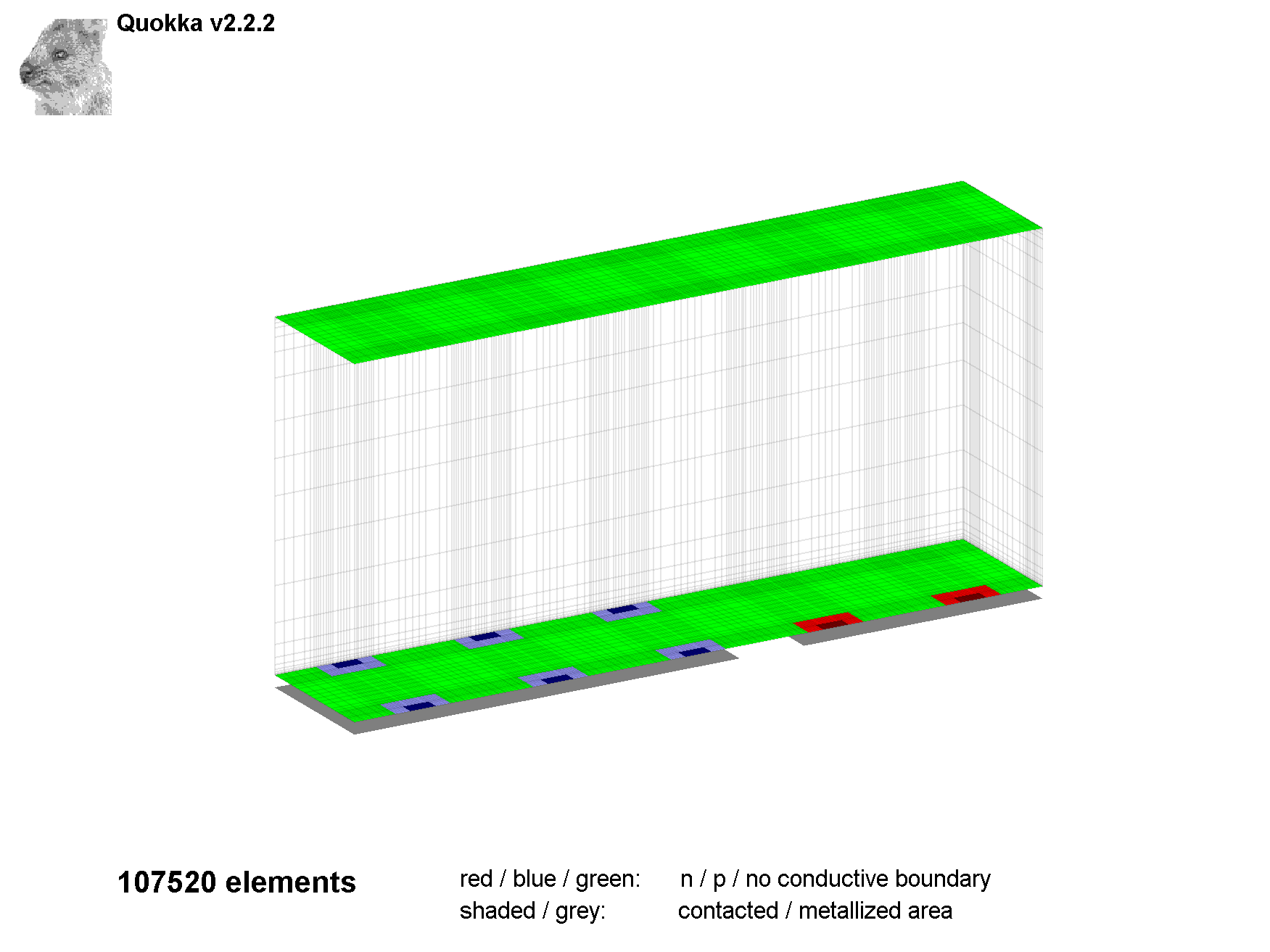
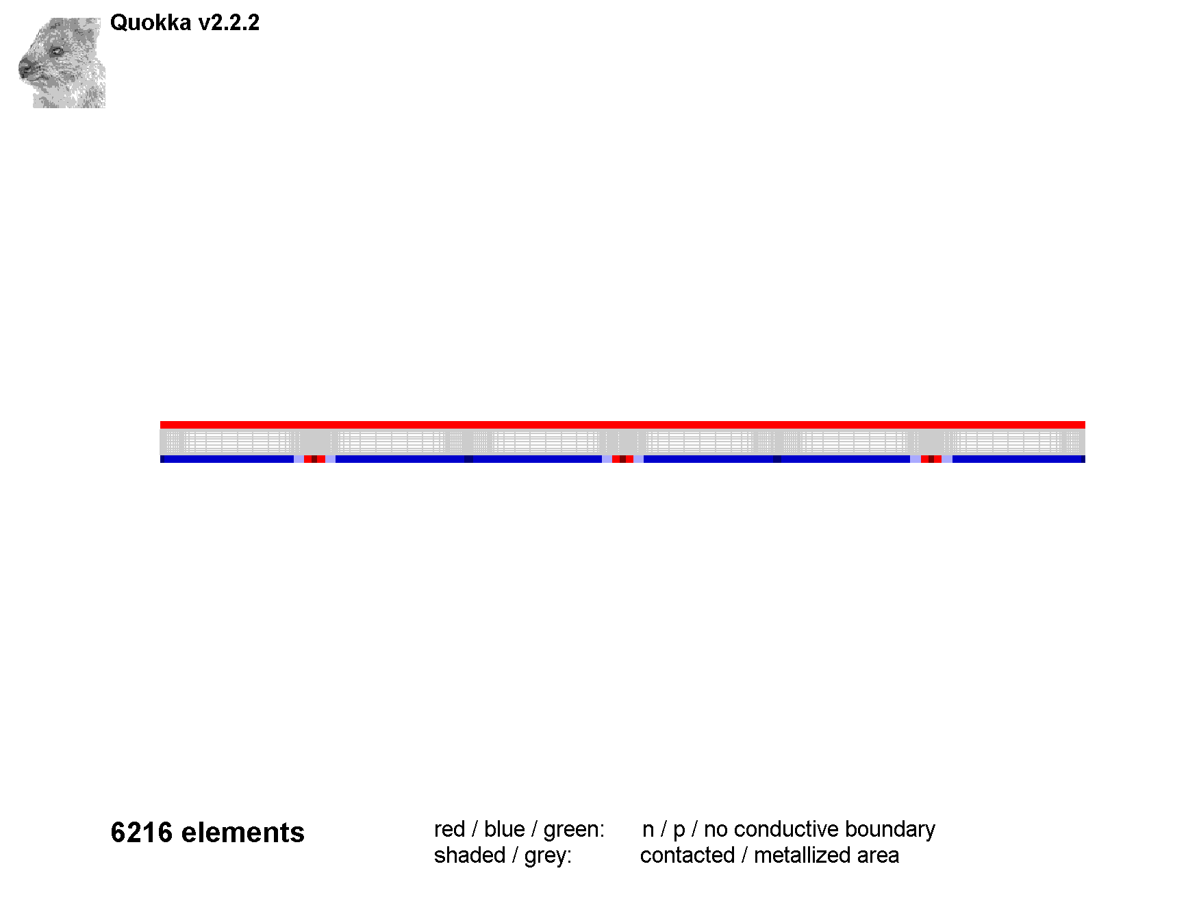
Figure 4: Example IBC geometries produced by Quokka; upper left: large area p+ region (emitter) with localized circular n+ regions, and localized contact openings; upper right: point-contact design; lower: large 2D solution domain containing multiple repetitions of symmetry element.
6.1.2 Defining multiple boundary regions
Quokka allows to define an arbitrary number of conductive boundaries with different shapes and properties by indexing. In areas where conductive boundaries overlap, the one with the highest index is applied. Their centre position is always aligned to every contact at the respective side (front / rear for FRC, left / right for IBC). An exception exists in the IBC version: if the width of a conductive boundary is larger than the x-pitch of the respective contacts, it is centred at the respective edge of the solution domain (left / right). Adjacent conductive boundaries of the same type are electrically connected. In regions where no conductive boundary is applied, properties for the non-conductive boundary are applied. Figure 5 illustrates this functionality.
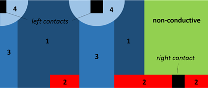
Figure 5: (non-sensible) example to illustrate definition of multiple conductive boundaries; IBC rear side with opposite contact positions and 4 conductive boundaries, one 'right' (#2: n+ BSF) and 3 'left' conductive boundaries (#1, #3, #4: p+ emitter); boundaries #1 and #2 are wider than the respective contact pitch and are therefore centred at the left and right solution domain edge, respectively, whereas boundaries #3 and #4 are centred at the respective contacts.
6.1.3 Meshing insights
Quokka uses an orthogonal, non-equidistant mesh for discretization of the solution domain, which is well suited for the typically cuboidal shapes of silicon solar cell devices. The automated meshing algorithm works as follows: first, a minimum element size in each coordinate direction is determined from the minimum of either the user input or the minimum feature / gap size divided by a user-defined scale factor. This minimum element size is applied to all feature edges, including front and rear side, but NOT the symmetry sides. From there the mesh is inflated where the size of adjacent elements is increased by the inflation factor. Typical settings for scale factor, inflation factor and minimum element sizes are pre-defined in the mesh-quality settings 1 (coarse), 2 (medium) and 3 (fine), and can further be defined by the user. Note that for many purposes a 'coarse' mesh will yield acceptably accurate results, and is the recommended initial setting due to numerical speed and robustness. However, mesh independency should be verified for sensitive results, see Verify Accuracy.
A complication arises when different junction depths for conductive boundaries are defined. The physical solution domain in Quokka covers the quasi-neutral region only, i.e. excludes the junction depths. At the same time the cuboidal solution domain can only accept a unique value for its size in z-direction. Quokka handles this by setting the solution domain size to the defined thickness less the area-average junction depth, see Figure 6. Care is taken to use the originally defined junction depths when calculating the generated and collected current in the boundary, and compensating for the spatial gap / overlap by accordingly adjusting the generation in the bulk next to the boundary. This approach is accurate if the junction depths are much smaller than the device thickness and the size of the conductive boundaries.
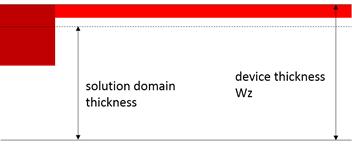
Figure 6: Illustration of solution domain thickness reduction by the area-average junction depth.
6.1.4 Both polarity contacts are always required
The solver algorithm in Quokka requires a voltage to be applied, which makes the definition of both polarity contacts a fundamental requirement . Often it is desirable to simulate test structures without contacts, i.e. lifetime or photo-luminescence test structures. This can still be done in Quokka by defining 'virtual contacts' and solving for open circuit conditions. If the properties of the virtual contacts are defined in a way that they represent non-contacted regions, their influence at open circuit eventually vanishes and the simulation represents a sample without any contacts. This is achieved by setting recombination of the contacted region equal to the non-contacted region it represents, and choosing a small contact size to not significantly supress lateral gradients by pinning the respective quasi-Fermi-potential to the constant voltage of the boundary. However, the virtual contact should not be too small to prevent extremely small element sizes and consequently high computational effort. A typically good value for the size of the virtual contact is a few percent of the solution domain size.
6.2 Varying input parameters: sweep and optimizer
6.2.1 Sweep
Quokka has the built-in functionality to perform parameter sweeps. It can sweep one or two independent groups of dependent parameters indexed. Here, dependent parameters mean that both must have the same number ofvalues, which is the number of simulations to be performed using the defined value pairs, and are indexed in the settings file by curly brackets {i}. For the two independent groups of parameters in contrast, each value of the first parameter group will be combined with each value of the second parameter group. For example, if each of the parameters in the first independent group has 5 values assigned sweep.values_1{1}=[v1 v2 v3 v4 v5], and 4 in the second independent group sweep.values_2{1}=[v6 v7 v8 v9], a total of 5x4=20 simulations will be performed. Either of the two independent groups can be disabled by assigning an empty matrix to its values, e.g. for disabling the second group: sweep.values_2{1}=[].
Sweep parameter can be any parameter assigned in the settings file, with the exception of some parameters with string values, in particular external filenames.
If the parallel mode is in, a sweep will be simulated in parallel, see Command Line Options.
6.2.2 Optimizer
Inbuilt in Quokka is a generic optimizer algorithm, essentially using Matlab′s bounded nonlinear optimizer algorithm′s, which allows to fit unknown input parameter(s) to known output characteristics. For a successful optimization, a careful setup is required as with any other such complex function to optimize, see Optimizer.
There are two different optimizer modes. Mode 1 allows to define multiple goal values to achieve, or one goal to maximize / minimize. For a minimize / maximize goal the number of unknown parameters can be more than one. Otherwise the number of unknown parameters have to be equal or less than the number of goals, where in the latter case least-square fitting is performed rather than attempting exact goal achievement. Mode 2 performs curve fitting, where the simulated curve will be fitted by least squares to a user-defined curve. This is most commonly done in conjunction with curve terminal conditions to produce the desired curve (IV, effective lifetime curve by suns-Voc, to), while the sweep functionality can also be used to produce the desired curve.
Another functionality within the optimizer is given by the 'override parameters'. This is needed when other input parameters are dependent on the unknown parameter, and need therefore be adjusted during the iterative optimization. For example, if one wanted to fit front and rear J0 of a symmetric lifetime structure, one would define only the front J0 as the unknown parameter, and override the rear J0 with the front J0 to ensure a symmetric structure for each simulation.
A second application for those overrides is to envoke 'sequential optimization' to perform multiple identical optimization tasks with different conditions. In the above example, one might want to investigate the influence of the wafer thicknesses on the derived J0. For this, the override can be used to assign multiple values to any input parameter other than the unknown one, and Quokka will perform the defined optimization for each of those values. Alternatively / additionally start, bound and goal inputs can be assigned multiple values (with the same number) to perform sequential optimization. Note that sequential optimization can NOT be envoked by the sweep functionality, as the optimizer is implemented 'on top'. Such a sequential optimization is performed in parallel, when the parallel mode is on, see Command Line Options.
7. Troubleshooting / FAQs
Table 6: Common problems with suggested solutions and / or explanations
| Problem / question | Solution / description |
|---|---|
| Inconsistent ni,eff and J0 |
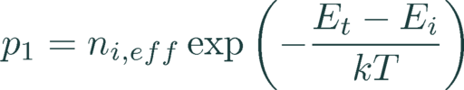
While (bulk-) ni,eff does actually have little direct impact on most important results like IV-characteristics, it can indirectly show large influence in combination with “J0” boundary recombination. The user must take care that a consistent assumption for ni,eff for both deriving J0 and for the subsequent device simulation is used. J0 values can often be adjusted to a different ni,eff by the assumption of J0⁄ni,eff2 = const, well valid for diffusions.
As the most prominent example, the Excel spreadsheets on Sinton lifetime testers typically assume ni,eff = 8.6e^9 cm-3 when calculating J0 values, which results in ca. 30% underestimation of recombination when the same J0 values and default ni,eff settings in Quokka are used at 300K. |
| Quokka stuck / bad or no convergence |
In estimated 95% of cases this is caused by a mistake in the settings or by setting very untypical conditions for a solar cell, not being reported by Quokka as such. Below is a list of common cases leading to convergence problems. If you still think Quokka should be able to solve your setup, please contact support@pvlighthouse.com.au.
|
| Cryptic error message | Not being the fun part and lacking commitment within a free tool, the implementation of error handling is far from comprehensive and a “cryptic error message” is the dominant behaviour when something goes wrong. Mostly this is due to errors in the settings file. If you created / changed it manually, a convenient way for a sanity check is uploading it to the settings file generator, which might find and fix wrong or missing assignments. If you can’t find anything wrong with your settings file, please send it to support@pvlighthouse.com.au. |
| Should I use ‘S’ or ‘J0’ model for surface recombination? | Which model is more appropriate is up to the user to decide and depends on the detailed physics within the near-surface region. As a simple guide, most highly doped regions or highly charged surfaces follow a J0 recombination, while some passivated surfaces are well approximated by an effective surface recombination velocity. In low injection, both models yield equivalent results. For low and moderately charged surfaces, neither of the two models may be applicable, and an analytic expression for the actual injection dependence needs to be used. |
| What exactly do the inputs suns and intensity do? |
Once a generation profile is defined by either of the generation types, it is scaled by the user input for suns, which therefore effectively states a scaling factor. However, further influence is given on the post-calculated efficiency as it also scales the intensity.
The user input for intensity does have no influence on the generation. It is solely required to post-calculate the efficiency. Furthermore, the intensity user input will be disregarded in the ‘1D_model’, as it is then defined by the chosen spectrum. The formula below highlights the influence of suns and intensity on the efficiency: efficiency = terminal power / (intensity × suns) A complication arises when one wants to scale an external generation profile to fit a desired current. Using the suns-value does this job, but also scales the intensity for calculating the efficiency, which is consequently not the desired (but physical correct) value. Therefore suns should not be used for this purpose, but rather generation.Jgen_correction should be enabled with the desired generation current defined as generation.Jgen. |
8. Quokka physics overview
© 2014 Andreas Fell
Quokka numerically solves the 1D/2D/3D steady-state charge carrier transport in a quasi-neutral silicon device in an efficient and fast manner. It uses so called 'conductive boundaries' to account for increased lateral conductivity in near surface regions (e.g. diffusion or inversion layer) and thus to simulate most silicon solar cell devices without major loss of generality. This page summarizes the implemented models and material properties.
8.1 Charge carrier transport model
The equations here are shown for a p-type bulk as an example, and can be analogously derived and applied for an n-type bulk.
8.1.1 Volumetric (bulk) equations
The basic equations solved in Quokka are a simplified set of two differential equations describing the steady-state charge carrier transport in a quasi-neutral semiconductor. The variables to solve for are the quasi-Fermi potentials of electrons and holes φFn and φFp respectively.
 (1)
(1)
 (2)
(2)
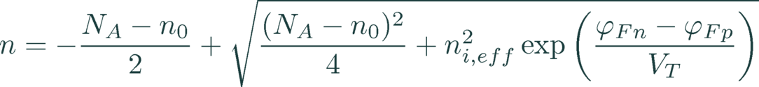
The conductivities and the recombination rate in general is a function of the carrier density. They can be derived from the quasi-Fermi potentials by the quasi-neutrality condition p ≈ n + NA - n0 and equation (18) to [1]:
 (3)
(3)
8.1.2 Boundary conditions
Boundary recombination
For both conductive and non-conductive boundaries, the recombination current at or into the boundary is evaluated by either a J01/J02 model, S model, or a user-defined analytic expression.
 (4)
(4)
 (5)
(5)
 (6)
(6)
Symmetry boundaries
At the symmetry boundaries, i.e. all boundaries except the front and the rear side, the component of the gradient of the quasi-Fermi potentials in direction of the surface normal, defined by the normal vector
 , is zero:
 (7)
(7)
Non-conductive boundaries
The electron current equals the negative recombination current:
 (8)
(8)
At non-contacted regions the total current into the boundary needs to be zero:
 (9)
(9)
An electrical contact with the voltage V at the non-conductive boundaries is included by setting the current density through the contact resistance rc equal to the total current density at the boundary:
 (10)
(10)
At regions without external contacts the contact resistance becomes infinite and sets the total current density into the boundary consistently to zero. Care should be taken when simulating a lowly recombining contact, as the quasi-neutrality approximation is not valid when significant currents are extracted and can thus result in significant errors.
Note that this implementation of the contact resistance, also in case of a conductive boundary, accounts correctly for current transfer effects into the contacts.
Conductive boundaries
The conduction of carriers in a conductive layer at the surface (e.g. diffusion or inversion layer) is accounted for by a 2D continuity equation of the majority quasi-Fermi potential φFdiff with the sheet resistance Rsheet.
 (11)
(11)
For a n-type conductive boundary (emitter) this gives the boundary condition for the bulk electron quasi-Fermi potential:
 (12)
(12)
The source term Jdiff equals the total current density from the base into the emitter less the current density into the contact:
 (13)
(13)
The hole current density into the boundary equals the recombination current density less the current density generated within the boundary JG times its collection efficiency ηcoll, which gives the boundary condition for the hole quasi-Fermi potential:
 (14)
(14)
For a p-type diffusion (back surface field) the expressions are equivalent with altered carrier types and an inverted sign of the recombination current density.
8.2 Silicon properties
8.2.1 Band structure and intrinsic carrier density
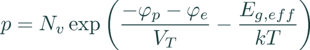
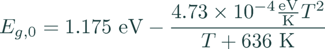
The effective band gap energy is calculated by a temperature dependent Eg,0 and a doping dependent band gap narrowing (BGN) ΔEg.
 (15)
(15)
ΔEg is determined by a lookup table with values derived from [2] which considers a doping dependence at 300 K only, i.e. representing the curve in Fig. 9 of [2].
To calculate carrier densities Boltzman statistics are assumed. This is valid as Quokka solves only in the relatively lowly doped bulk, where the difference to Fermi-Dirac statistics is negligible.
 (16)
(16)
 (17)
(17)
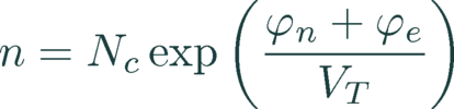
Here φn and φp are the electron and hole quasi-Fermi potentials, Nc and Nv the density of states (DOS) in the conduction and valence band respectively, and VT = kT/q the thermal voltage. Note that what is denoted as the electric potential φe is more accurately the conduction band edge potential, which differs to the electric potential by the electron affinity and the reference electric potential.
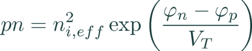
It follows the well-known relation between pn product and Fermi-level splitting which is applied to solve the bulk carrier transport, with the effective intrinsic carrier density ni,eff2 being the only decisive value for accurate modelling of carrier transport.
 (18)
(18)
 (19)
(19)
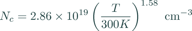
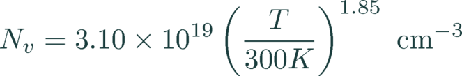
As default settings Quokka uses the values for DOS published by Green [3], and the temperature dependent band gap expression given in the Sentaurus user manual with slightly changed parameters to match the commonly accepted best value for the intrinsic carrier density at 300 K, ni,0=9.65 × 109 cm-3.
 (20)
(20)
 (21)
(21)
 (22)
(22)
8.2.2 Carrier conductivity
The conductivities σ of the carriers are functions of their mobilities μ.
 (23)
(23)
 (24)
(24)
Implemented in Quokka are the mobility models by Klaassen [4] and Arora [5], where in the latter case the excess carrier density is added to the doping density to account for injection dependence, which is the way it is implemented in PC1D.
8.2.3 Bulk recombination
Quokka accounts for radiative, Auger and Shockley-Read-Hall (SRH) recombination in the bulk to calculate the recombination rate R. The sum of radiative and Auger recombination is called intrinsic recombination. The Auger models implemented in Quokka comprise the parameterizations by Kerr and Cuevas [6], Altermatt [7] and Richter et al. [8] (eq. (18) without Brel), as well as the constant recombination coefficient model by Sinton and Swanson [9], which is the one used in the spreadsheet of the Sinton testers.
Implemented in Quokka is the general SRH expression:
 (25)
(25)
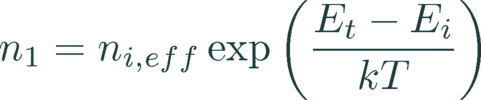
Multiple custom defects can be defined by their defect level Et relative to the intrinsic energy Ei (approx. defined as the energy level in the middle of the effective bandgap), the capture cross sections cn/p and the defect density Nt, with the thermal velocity vth = 1.1 × 107 cm s-1.
 (26)
(26)
 (27)
(27)
 (28)
(28)
Additionally a simplified midgap defect energy recombination is implemented where the user inputs τp0/τn0, and n1/p1 are equal to ni,eff.
As a further contribution is given by the boron-oxygen recombination in p-type material as given by Altermatt [7], where the user needs to set the oxygen concentration Nt,0 and a processing dependent parameter m while the boron concentration is given by the doping density NA and the energy level is 0.41 eV below the conduction band edge.
 (29)
(29)
 (30)
(30)
The last contribution to bulk recombination is by a fixed, i.e. injection independent, minority carrier lifetime τb,fixed. The total bulk recombination is then calculated as the sum of all contributions, where each contribution can be either switched off, or needs to be assigned very high lifetime values to effectively disable:
 (31)
(31)
8.2.4 Optical absorption
Wavelength dependent refractive index / absorption data is required for determining the generation profile when the ‘1D_model’ is used, as well as for re-absorption within luminescence modelling. By default, Quokka uses the optical properties of silicon from Nguyen [10], and combines it with the data from Green [11] to cover the full wavelength range. Quokka incorporates the published temperature dependence for deriving optical properties at arbitrary temperatures. As a further option, which is prominently used in literature and other software tools, the data from Green [11] fixed at 300K can be set.
8.3 Optical modelling by '1D_model'
Quokka’s focus in on the simulation of carrier transport and excludes the capability to perform optical modelling from physical optical properties of the cell and consequently derive the required generation profile. There are several options to define generation, comprising the direct definition of the generation profile by the user, a user-defined generation current, and a one-dimensional model accounting for wavelength-dependent effective properties, which was published in [12].
The one-dimensional model ‘1D_model’ derives a generation profile from a defined spectrum, front transmission Tfront(λ) and pathlength enhancement Z(λ). Note that those inputs already define the total generation current (for a given wafer thickness Wz and refractive index data of silicon). Consequently total generation can be considered a user-input rather than a quantity modelled by Quokka, which ensures consistency with for example raytracing programs when deriving the required inputs. Furthermore, the facet angle of the front surface texture must be given, which is zero for a planar surface.
For each wavelength bin (5nm in Quokka), the incoming photon flux Nph(λ) is derived from the incident spectrum. Each monochromatic ray is then traced through the wafer accounting for its angle to enhance its travel length and absorption. For a textured surface, a different angle is applied inside and outside of the junction depth as suggested in [13], see figure below. After traveling to the rear of the wafer, the remaining absorption from the difference of total pathlength and first-pass pathlength is equally distributed throughout the thickness of the device. It has been found that this model provides high accuracy for wafer-based silicon solar cells.
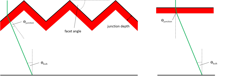
Figure 7: Illustration of ‘1D_model’ generation calculation; left: textured case; right: 1D representation.
8.4 Free energy loss analysis (FELA)
The free energy loss analysis (FELA) as comprehensively described in [14] is implemented in Quokka. It enables to compare resistive losses and recombination losses in the common power loss unit mW/cm². Incidentally, for the typical 100 mW/cm² incident light intensity, the power loss values are equivalent to efficiency loss in %abs.
A drawback of the FELA is that recombination losses are in general underestimated, as they are a function of quasi-Fermi level splitting, which in turn is a result of recombination. The losses add up to the generated power density, which is also a function of quasi-Fermi level splitting and therefore overall recombination. Effectively, the part of the entropy loss which is caused by avoidable recombination is missing in FELA when aiming for a loss breakdown towards the Auger-Limit [15]. However, FELA is very suitable to identify the main resistive and recombination loss contributions and the potential for incremental efficiency improvements. Table 1 summarizes the expressions used for the different loss contributions considered in Quokka.
A notable quantity Quokka calculates is the FELA balance εFELA. Mathematically the output power must equal the generated power less the sum of the FELA contributions. The FELA balance gives a metric how close this is numerically achieved, and is consequently a useful indicator for the consistency and accuracy of the numerical solution to the carrier transport equations. See the user manual for details on how this should be interpreted. It is defined as
 (32)
(32)
Table 7: FELA expressions; A denotes the lateral (xy) solution domain area, ∆φ the splitting of quasi-Fermi potentials, dV volume integration and dA boundary integration
| FELA name / comment | Equation |
|---|---|
| generated power |  |
| bulk recombination loss |  |
|
boundary recombination loss including suboptimal collection efficiency loss for conductive boundaries |
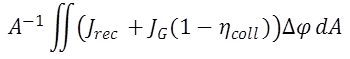 |
| bulk electron resistive loss | 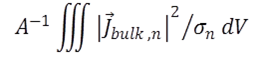 |
| bulk hole resistive loss | 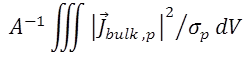 |
|
conductive boundary resistive loss note that boundary current density has units of A/m, opposed to A/m² in the bulk |
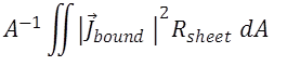 |
|
contact resistance loss takes current transfer effects into account |
 |
| external shunt resistance loss | Vuc2 / Rshunt |
| external series resistance loss | Jterm2Rseries |
| external diode loss | VucJD |
8.5 Luminescence modelling
8.5.1 Fundamental equation
Quokka 2.0 simulates the detected luminescence map by integrating over the z axis of the simulated device:
 (33)
(33)
where rsp is the rate of spontaneous emission via band-to-band transitions in silicon, fesc the escape function defining the probability that a photon will be emitted from the device and Φ the detector sensitivity. As Quokka separates the electrical and optical simulations, luminescence maps can be produced under either photoluminescence or electroluminescence conditions. Each component of Equation ( 31 ) is described in detail in the subsequent sections.
8.5.2 Spontaneous emission spectrum
The rate of spontaneous emission via band-to-band transitions is calculated using the generalized form of Planck's Law as described by Wurfel [16]. The rate of spontaneous emission (in units of photons nm-1 s-1 cm-2) emitted isotropically into 4π steradians is expressed as:
 (34)
(34)
where αSi(λ) is the wavelength-dependent absorption coefficient of silicon, BB(λ,T) the black-body photon flux and Δη(x,y,z) = φFn - φFp the local separation of the quasi-Fermi energies. Quokka employs the optical data of Daub over the wavelength range of the emission spectrum of silicon as it has demonstrated the best fit to experiment [17]. The electronic simulation of Quokka calculates the local splitting of the quasi-Fermi potential for every element of the device and from Equation ( 32 ), an accompanying radiative emission rate, an example of which is produced in the figure below.
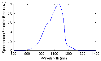
Figure 8: Emission spectrum.
This spectrum, however, is not what is ultimately emitted from the silicon wafer or solar cell, which is determined by the optical losses within the structure.
8.5.3 The escape function fesc
Numerous so-called emission functions exist in literature. Several [18-20] have been implemented in Quokka. These functions describe the probability with which a spontaneously emitted photon will escape from the emitting medium without being 'lost', either to reabsorption or total internal reflection.
In the case of perfectly planar devices, only a relatively small proportion of emitted photons fall within the narrow escape-cone that is determined by the relative refractive indices of the emitting and ambient media. In Quokka, it is assumed that the device is in an air ambient (nair(λ) = 1), and the fraction 1/nSi2 of total emitted photons falls within the escape cone.
If the device surfaces are perfectly planar and parallel, the photons incident on the silicon-air interface beyond the escape cone are totally internally reflected and assumed to be unavailable to an external detector. However, not all photons within the escape cone will be transmitted on their first interaction with the wafer surface and are instead reflected internally. Owing to subsequent internal reflections these photons will have a further opportunity to be emitted from the front surface of the device, but on each pass will be attenuated by reabsorption in the silicon bulk modeled after Beer-Lambert absorption. This brings us to the escape function proposed by Schick [18], which is implemented in Quokka to describe the emitted luminescence flux for planar devices.
 (35)
(35)
It has been noted by Schinke et al. [20] that the escape function of Equation (33) is functionally equivalent to those described by Green [21], Daub [22] and Trupke [23], and thus is representative of a function broadly used in the PV literature.
Quokka also includes escape functions that account for diffuse and/or specularly reflecting surfaces. The model of Rudiger et al. [19] assumes that the front and rear surfaces of the device are fully diffuse reflectors, as might be encountered with front and rear textured devices. The escape function is described by:
 (36)
(36)
The figure below plots the emitted luminescence spectrum simulated by Quokka for the escape functions of Schick and Rudiger.
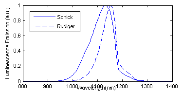
Figure 9: Emission spectra modelled after the escape functions of Schick and Rudiger.
A more general escape function has been developed by Schinke et al. [20], which describes the probability of photon emission for any combination of planar (specular) and textured (diffuse) reflecting surfaces. It contains the functions of Schick and Rudiger as special cases, determined by appropriate input variables. It has been implemented in Quokka, with the functions of Schick and Rudiger retained for the relative ease of use. For details on the general emission function, refer to [20], which also provides a valuable overview of escape functions employed in the PV literature.
It is important to note that the above escape functions are statistical predictions of emission, and do not account for the spatial distribution of the emitted photons. Thus, luminescence maps, particularly in the case of diffusely reflecting samples, need to be interpreted with caution. Quokka assumes that the emitted photons are constrained within the z-axis of the element from which they are emitted.
8.5.4 Geometrical blurring model
To address this last mentioned limitation, the geometrical blurring model by Padilla et al. [24] is implemented in Quokka and can be chosen instead of the escape functions. It assumes both the front and the rear internal surfaces to be Lambertian reflectors. Note that it requires a relatively fine lateral mesh to give accurate and smooth results, which, in particular in 3D, can be highly computationally expensive.
8.5.5 The detection function Φ
The detection function describes the wavelength-dependent external quantum efficiency (EQE) of the imaging sensor, including the presence of any short or long-pass filters. The response is modelled after Beer-Lambert absorption assuming perfect collection efficiency for absorbed photons. Quokka will determine the QE for a silicon-based detector of user-defined thickness, or will accept a definition of the sensor's EQE via an external excel spreadsheet.
8.6 External circuit
Below is a sketch of the external circuit elements and current directions. The convention is that a positive unit cell voltage Vuc in dark condition results in a positive unit cell current Juc, regardless of whether it is a n-type or p-type solar cell, and Vuc is applied to the contact of opposite polarity to the bulk. The external diode is in forward bias and its current is given by the saturation current density J0D and the ideality factor nD.
 (37)
(37)
Figure 10: External circuit model.
8.7 Quantum efficiency
Quokka has an inbuilt algorithm to derive a biased quantum efficiency curve. First, using the bias illumination only, short circuit current conditions are searched for iteratively. Note that this does not mean actual short circuit conditions, but searching for a higher unit cell voltage which still results in a negligible difference of extracted current to short circuit current Jsc,bias, which is usually the case up to a couple of 100 mV. The reason for this is to prevent numerical inaccuracies, which can be significant at actual short circuit. This so derived unit cell voltage is used as a fast to solve for fixed terminal condition for the following simulations. A monochromatic illumination is then added with a photon flux representing a small fraction of the bias generation current Jph=0.005 Jgen,bias and a sweep of the wavelength results in a wavelength dependent short circuit current Jsc(λ).
The fundamental quantum efficiency characteristic Quokka simulates is the collection efficiency CE(λ), which is largely independent of the optical properties of the device. The other more common characteristics internal and external quantum efficiency IQE(λ) and EQE(λ) are essentially derived from the collection efficiency by the optical input parameters front surface transmission Tfront and pathlength enhancement Z(λ). The respective formulas are given below, with the effective transmission Teff(λ) being defined as the (unshaded) front transmission times the unshaded area fraction Teff(λ) = Tfront(λ) Aunshaded⁄Atotal:
 (38)
(38)
 (39)
(39)
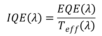 (40)
(40)
8.8 References
| [1] | A. Fell, "A free and fast three-dimensional/two-deimensional solar cell simulator featuring conductive boundary and quasi-neutrality approximations," IEEE Transactions on Electron Devices, 60, pp. 733–738, 2013. |
| [2] | A. Schenk, "Finite-temperature full random-phase approximation of band gap narrowing for silicon device simulation," Journal of Applied Physics, 84, pp. 3684-3695, 1998. |
| [3] | M.A. Green, "Intrinsic concentration, effective densities of states, and effective mass in silicon," Journal of Applied Physics, 67, pp. 2944-2954, 1990. |
| [4] | D.B.M. Klaassen, "A unified mobility model for device simulation - I. Model equations and concentration dependence," Solid-State Electronics, 35, pp. 953-959, 1992. |
| [5] | N.D. Arora, J.R. Hauser and D.J. Roulston, "Electron and hole mobilities in silicon as a function of concentration and temperature," IEEE Transactions on Electron Devices, 29, pp. 292-295, 1982. |
| [6] | M.J. Kerr and A. Cuevas, "General parameterization of Auger recombination in crystalline silicon," Journal of Applied Physics, 91, pp. 2473-2480, 2002. |
| [7] | P.P. Altermatt, "Models for numerical device simulations of crystalline silicon solar cells - a review," Journal of Computational Electronics, 10, pp. 314-330, 2011. |
| [8] | A. Richter, S.W. Glunz, F. Werner, J.Schmidt and A. Cuevas, "Improved quantitative description of Auger recombination in crystalline silicon," Physical review B, 86, 165202, 2012. |
| [9] | R.A. Sinton and R.M. Swanson, "Recombination in highly injected silicon," IEEE Transations on Electron Devices, 34, pp. 1380-1389, 1987. |
| [10] | H. T. Nguyen, F. E. Rougieux, B. Mitchell, and D. Macdonald, "Temperature dependence of the band-band absorption coefficient in crystalline silicon from photoluminescence," Journal of Applied Physics115, pp. -, 2014. |
| [11] | M.A. Green, "Self-consistent optical parameters of intrinsic silicon at 300 K including temperature coefficients," Solar Energy Materials and Solar Cells, 92, pp. 1305-1310, 2008. |
| [12] | A. Fell and K. R. McIntosh, "Deriving the generation profile for silicon solar cells from lumped optical parameters," in 42rd IEEE Photovoltaic Specialists Conference, New Orleans, USA, 2015. |
| [13] | P. A. Basore, "Numerical modeling of textured silicon solar cells using PC-1D," Electron Devices, IEEE Transactions on, vol. 37, pp. 337-343, 1990. |
| [14] | R. Brendel, S. Dreissigacker, N. P. Harder, and P. P. Altermatt, "Theory of analyzing free energy losses in solar cells," Applied Physics Letters, vol. 93, pp. 173503-173503-3, 2008. |
| [15] | J. Greulich, H. Höffler, U. Würfel, and S. Rein, "Numerical power balance and free energy loss analysis for solar cells including optical, thermodynamic, and electrical aspects," Journal of Applied Physics, vol. 114, pp. -, 2013. |
| [16] | P. Wurfel, S.Finkbeiner and E. Daub, "Generalized Planck's radiation law for luminescence via indirect transitions," Applied Physics A, 60, pp. 67-70, 1995. |
| [17] | B. Mitchell, M.K. Juhl, M.A. Green and T. Trupke, "Full spectrim photoluminescence lifetime analysis on silicon bricks," IEEE Journal of Photovoltaics, 3, pp. 962-969, 2013. |
| [18] | K. Schick, E. Daub, S. Finkbeiner and P. Wurfel, "Verification of a generalized Planck law for luminescence radiation from silicon solar cells," Applied Physics A, 54, pp. 962-969, 2013. |
| [19] | M. Rudiger, T. Trupke, P. Wurfel, T. Roth and S.W. Glunz, "Influence of photon reabsorption on temperature dependent quasi-steady-state photoluminescence lifetime measurements on crystalline silicon," Applied Physics Letters, 92, 222112, 2008. |
| [20] | C. Schinke, D. Hinken, J. Schmidt, K. Bothe and R. Brendel, "Modeling the spectral luminescence emission of silicon solar cells and wafers," IEEE Journal of Photovoltaics, 3, pp. 1038-1052, 2013. |
| [21] | M.A. Green, "Analytical expressions for spectral composition of band photoluminescence from silicon wafers and bricks," Applied Physics Letters, 99, 131112, 2011. |
| [22] | E. Daub and P. Wurfel, "Ultra-low values of the absorption coefficient for band-band transitions in moderately doped Si obtained from luminescence," Journal of Applied Physics, 80, pp. 5325-5331, 1996. |
| [23] | T. Trupke, E. Daub and P. Wurfel, "Absorptivity of silicon solar cells obtained from luminescence," Solar Energy Materials and Solar Cells, 53, pp. 103-114, 1998. |
| [24] | M. Padilla, H. Höffler, C. Reichel, H. Chu, J. Greulich, S. Rein, W. Warta, M. Hermle, and M. C. Schubert, "Surface recombination parameters of interdigitated-back-contact silicon solar cells obtained by modeling luminescence images," Solar Energy Materials and Solar Cells, 120, pp. 363–375, 2014. |