 (A.1)
(A.1)This section describes the isolated-element approach used within PC1D to obtain rapid, accurate solutions of the semiconductor transport equations. The emphasis in this program has been on reliable convergence for a broad range of doping profiles and boundary conditions.
The five semiconductor equations (Section A.1) can be readily reduced to three equations in three unknowns. There are several options for selecting the solution variables; none appears to have a significant advantage. For PC1D we have chosen the electrostatic potential, y, and the electron and hole quasi-Fermi potentials, fn and fp. Three expressions are required at each interface between elements. Poisson's equation minimizes the total electrostatic energy in the adjoining elements, and both electron and hole currents must be continuous across each interface.
A.1 Fundamental Equations
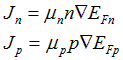
The numerical method of PC1D uses the two-carrier semiclassical semiconductor transport equations. These equations are derived from the Boltzmann transport equation with the following assumptions: the two carriers flow independently (no carrier-carrier scattering), both carrier populations remain in thermal equilibrium with the surrounding crystal lattice (no hot carriers), the mobility of carriers is isotropic, and the structure of the energy levels available to electrons is not significantly affected by excitation (rigid bands). The effect of magnetic fields is also neglected and the device temperature is assumed to be uniform. The resulting equations for electron and hole current density (Jn, Jp) are commonly written in terms of the electron and hole density (n, p), the electron and hole mobility (mn, mp), and the electron and hole quasi-Fermi energies (EFn, EFp).
(A.1)
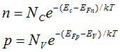
The quasi-Fermi energies relative to their corresponding energy band define which of the energy states available to electrons are filled by carriers from each population, thereby determining the local concentration of both carriers. For non-degenerate material, the Boltzmann exponential approximation to the Fermi distribution function can be utilized:
 (A.2)
(A.2)
Here Nc and Nv are the effective density of states in the conduction and valence bands. Ec and Ev are the energy levels of the two band edges. The effects of degenerate doping can be included in this Boltzmann-like form by modifying Ec and Ev. Degeneracy due to high injection levels is not included in this treatment.
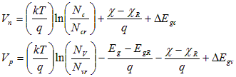
Define the quasi-Fermi potentials (fn, fp) as the separation of the quasi- Fermi energies relative to the equilibrium Fermi energy at some selected reference location. For PC1D, this location is taken as x=0. The position of the two band edges in Eq. (A.2) relative to this reference energy depends on the electrostatic potential and any spatial variation in the band structure. To describe variations in the band structure, two band-edge potentials are introduced, Vn and Vp. These potentials represent the shift (toward the centre of the bandgap) of the conduction and valence band edges with respect to the conditions at the reference location, after accounting for electrostatic effects. These shifts may be caused by spatial variations in material composition or bandgap narrowing due to heavy doping. Specifically, for bandgap Eg, electron affinity c, effective conduction (valence) band density of states Nc (Nv ), and conduction (valence) bandgap narrowing DEgc (DEgv),
 (A.3)
(A.3)
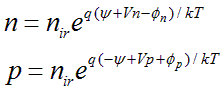
where q is the magnitude of the elementary electronic charge. The material (conduction and valence band) properties at the reference location can serve to establish a convenient zero reference for the electrostatic potential. Let zero electrostatic potential correspond to neutral intrinsic conditions in this material. Introducing these definitions into Eq. (A.2) produces a new pair of Boltzmann-like expressions for n and p,
 (A.4)
(A.4)
Here, nir is the intrinsic carrier concentration at the reference location.
Combining Eqs. (A.1) and (A.4) it is possible to eliminate n and p, expressing the two unknown current densities in terms of the two unknown quasi-Fermi potentials and the unknown electrostatic potential. All other parameters can be expressed in terms of these unknown quantities for a given device structure, providing two equations for five unknowns.
Two additional equations can be generated by accounting for the fate of all electrons and holes that enter a given volume of space. These continuity equations account for flow into the volume, creation of carriers within the volume (generation), and annihilation of carriers within the volume (recombination).
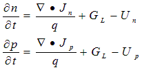 (A.5)
(A.5)
Here GL is the volume generation rate of electron-hole pairs due to the absorption of light (photogeneration), and Un, Up are the net volume recombination rates for electrons and holes.
The photogeneration model in PC1D includes a number of sophisticated features, including light trapping and free-carrier absorption. It does not consider the generation of multiple carrier pairs by energetic photons, two-photon absorption processes that use a trap level as an intermediate step, or absorption of photons created during radiative recombination. PC1D also does not include generation of carriers due to impact ionization, and thus will not predict avalanche breakdown.
A consequence of the two-carrier model is that electrons and holes are always created and annihilated in pairs, so that Un= Up= U. This approximation is valid only for high-quality material in which the concentration of occupied trap states is small compared with the carrier populations. The net recombination (U) can, in turn, be expressed in terms of the three unknown potentials (y, fn, fp). The recombination model includes trap-assisted, Auger, and band-to-band processes. Other factors must be neglected for reasons of computational efficiency, including changes in the trap cross-sectional area or energy level as a function of occupation state, and the effect of traps distributed throughout the bandgap.
The addition of Eq. (A.5) makes it possible to eliminate Jn and Jp as unknowns, leaving two equations in the three unknown potentials. Poisson’s equation of electrostatics provides the third and final independent equation.
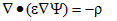 (A.6)
(A.6)
where r is the volume charge density and e is the permittivity. Contributions to the charge density include the electron and hole densities and the concentration of ionized donor and acceptor impurities. The two- carrier model neglects the charge associated with trap states located within the bandgap. PC1D assumes that all of the available dopants are ionized. This is an adequate assumption at room temperature and above, especially since the true dopant concentration is rarely known with great accuracy. At lower temperatures, the user must adjust the doping profiles to represent only the ionized dopant density.
As with any set of differential equations, boundary conditions represent an essential component in defining a unique solution. For the semiconductor transport equations, three boundary conditions are required at each external surface. A variety of boundary conditions can be used. Most analytical models assume that (1) the majority-carrier concentration is fixed at its equilibrium value, (2) the minority-carrier concentration is related to the minority-carrier current density by a surface recombination velocity, and (3) the surface electrostatic potential is shifted from its equilibrium value by an amount equal to the externally-applied voltage. These conditions are appropriate when all surfaces are heavily doped and electrically contacted, either directly or indirectly.
A more general set of boundary conditions is used in PC1D to accommodate lightly doped and insulated surfaces. The three boundary conditions at each surface are based on (1) injected current density, (2) surface recombination, and (3) surface electrostatic potential. The injected total current density is zero at insulated surfaces, and is controlled by the external circuit at contacts. PC1D provides two surface recombination models: a Shockley-Read-Hall recombination velocity model that permits separate electron and hole velocities through a trap level located anywhere in the bandgap, and a saturation current density model that gives a recombination rate proportional to the excess pn product at the surface. Three boundary conditions are available for the surface electrostatic potential: neutral surface charge density, the surface charge density remains at its equilibrium value, or the surface electric field remains at its equilibrium value. Constant surface charge density is appropriate at metal-semiconductor contacts, including Schottky contacts, whereas constant surface electric field is more appropriate at insulated surfaces.
At electrical contacts, PC1D allows the amount of injected current to be determined, in part, by the device being simulated. A Thevenin-equivalent circuit is attached to each electrical contact, consisting of a voltage source, series resistance, and external shunt elements. By varying the source resistance from a small value to a large value, the entire spectrum of boundary conditions ranging from fixed-voltage to fixed-current can be simulated.
A complication in applying the injected-current boundary condition arises when the contact itself is not a part of the solution region. It is often the case that a significant distance may lie between the contact and the solution region. Contacts to practical devices are made to heavily-doped material, so one can generally assume that the injected current will enter the solution region as majority-carrier flow spread throughout the region that matches the dopant type at the contact. To simplify matters, PC1D concentrates this majority-carrier current into a single injection point. The resulting electrostatic potential shift at the point of injection presumably causes a similar shift in the electrostatic potential near the contact. There will be a substantial difference, however, if the point of current injection in the solution region is in high-level injection. The difference in injection levels between the solution region and the contact produces an electrostatic potential difference across the intervening material, even when no current is flowing. For this reason, it is better to use the majority-carrier quasi-Fermi potential to determine the voltage at contacts. In the heavily doped material adjacent to the contact, the majority-carrier quasi-Fermi potential must shift in unison with any shift in the electrostatic potential in order to maintain a fixed volume charge density at the surface. Thus, the majority-carrier quasi-Fermi level is a valid indicator of the contact voltage, with the advantage that it does not differ significantly between the solution region and the contact. What difference might exist will be proportional to current and can therefore be modelled using the external series resistance.
A.2 Discretization
The first step in the numerical solution of the semiconductor equations described in Section A.1 is the discretization of the device, both in time and space. PC1D is a quasi-one-dimensional model, so the device is spatially divided into a finite set of M elements along a solution dimension "x", which approximately follows the direction of current flow in the device and is not necessarily a straight line. The dividing point between any two elements is called a node. The nodes are numbered from zero at the left boundary to M at the right. Subscripts of j or k are used to denote values at the jth or kth nodes, respectively. The cross-sectional area for current flow is a function of x, with a value Ak assigned to each node.
Poisson's equation is satisfied within this discrete space of elements by minimizing the total electrostatic energy of the system, We.
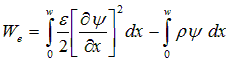 (A.7)
(A.7)
where w is the width (thickness) of the device. A minimization of this functional with respect to y, for a given charge distribution, r, gives the electrostatic potential. This minimization is achieved in a discrete sense by approximating y, r, and e. Both y and r are given a linear spatial variation within each element. The permittivity, e, is assumed to be uniform within each element. Setting the differential energy to zero yields the following discrete equation at each internal node k:
Poisson's Equation:
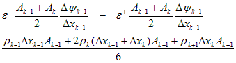 (A.8)
(A.8)
where e+ and e- refer to the permittivity of the elements on the right and left sides of the node, respectively. In Eq. (A.8), a delta notation is used to refer to the difference in a value across an element; that is, Dyk = yk+1 - yk, and Dyk-1 = yk - yk-1.
A second discrete equation at each node is based on the transport equation for electrons. Start with a quasi-one-dimensional version of Eq. (A.1), which gives the electron current, In, in the direction of the solution dimension.
 (A.9)
(A.9)
The mobility in Eq. (A.9) is electric-field dependent. The model used for this dependency is
 (A.10)
where E = - Ñy is the electric field intensity and vsat is the high-field saturation velocity, which may be different for electrons and holes. The denominator of Eq. (A.10) is assumed to be uniform within each element.
Define a modified electric potential, n(x).
 ,(A.11)
where mr and Ar are arbitrary fixed reference values for mobility and area. Substitute the potentials of Eq. (A.4) for n in Eq. (A.9) and rewrite the expression in terms of the modified potential of Eq. (A.11).
 ,(A.12)
Eq. (A.12) can be rearranged so that the quasi-Fermi potential is the only position-dependent value on the RHS of the equation.
 (A.13)
where Dr = mr·kT/q defines the reference diffusivity. A contour, or path, integral can be applied to both sides of this equation. The contour is taken across a single element, following the solution dimension x from the node at xk to xk+1.
 (A.14)
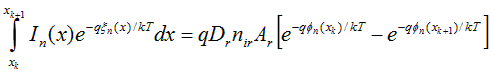 (A.15)
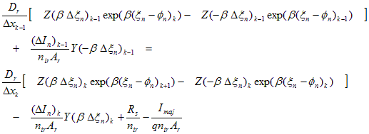
The value of this approach is now apparent. To complete the integration on the LHS of Eq. (A.15), it is only necessary to make assumptions regarding the spatial variation of two well-behaved variables: In and xn. No assumption regarding the spatial variation of on was necessary. Since the carrier concentration, n, depends on both xn and fn, this is equivalent to saying that no constraints have been imposed on the spatial variation of n within the element. If we assume that both xn and In vary linearly within each element, the integral can be performed to produce a direct expression for the electron current at the left edge of the element (node xk). Letting b be the inverse thermal voltage, q/kT, the following discrete equations result.
Electron Current Transport:
(A.16)
where Z(u) = u / (eu - 1) and Y(u) = ( 1-Z(u) ) /u
In Eq. (A.16), the net electron current leaving the element, DIn, is equal to the total rate of recombination within the element, minus the total rate of generation, plus the rate that electrons are accumulating as a function of time. In PC1D, photogeneration within each element is based on assuming a separate exponential absorption characteristic for each wavelength, the recombination rate is assumed to vary linearly with position across each element, and carrier accumulation is calculated assuming that the excess electron concentration is a linear function of position. The time dependence of the accumulation is calculated as a backward difference, assuming an exponential function of time unless the excess has changed sign since the last time step, in which case a linear time dependence is used.
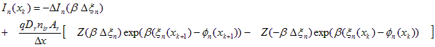
A similar derivation gives an expression for hole current, providing the third discrete equation needed at each node.
Hole Current Transport:
 (A.17)
A.3 System Solving
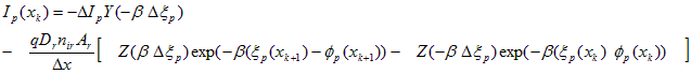
The electron and hole currents at node k can each be calculated independently for the two elements that adjoin at that node. Each carrier current should be continuous at the node except for interface recombination and majority-carrier current that may be injected at that node from an external source. Using the discrete expressions for carrier current developed in Section A.2, two equations at each internal node k result.
Hole Current Transport:
 (A.18)
Electron Current Transport:
 (A.19)
Eqs. (A.18) and (A.19), combined with Eq. (A.8), provide three simultaneous non-linear equations at each internal node. Added to these are three equations at each boundary that are based on (1) injected current density, (2) surface recombination, and (3) surface electrostatic potential. The first two of these boundary conditions are implemented using Eqs. (A.18) and (A.19), with the expression for current that extends beyond the boundaries of the device set to zero (ie. set LHS to zero at x=0). The electrostatic- potential boundary condition either equates the volume charge density at the surface to its equilibrium value (0 for a neutral surface), or equates the electric field at the surface to its equilibrium value. For M elements, there are a total of 3(M+1) equations for 3(M+1) unknowns.
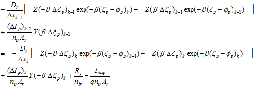
These non-linear equations are solved using Newton's method, which iteratively solves a sequence of linearized approximations of the equations. A Jacobian matrix is generated using the derivatives of each equation in terms of fn, y, and fp, each normalized by kT/q. The derivatives are calculated from analytical expressions for all terms except the surface and bulk recombination, which are calculated numerically based on a 1% change in the excess carrier densities. These expressions are such that the equations for node k involve only values from nodes k-1, k, and k+1. The resulting matrix has a numerical bandwidth of 11. The three equations are ordered so that the matrix will be diagonally dominant, eliminating the need for time-consuming pivoting. The electron current continuity equation is diagonal with fn, the hole current continuity equation is diagonal with fp, and the electrostatic equation is diagonal with y. A solution vector is constructed using the residual error from the 3(M+1) system equations. The entries for a single node are shown in Eq. (A.20).
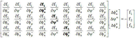 (A.20)
where superscripts -, o, and + correspond to values at nodes k-1, k, and k+1. The diagonal matrix components are shown in bold characters.
The Jacobian matrix is inverted using LU decomposition. Multiplying the factored Jacobian matrix times the solution vector generates a set of values for Dfn, Dy, and Dfp at each node. The electrostatic potential at each node is then updated using the following function, which puts a clamp on the amount the potential is allowed to change during a single iteration. The clamp value is supplied by the user. The default is 5 kT / q.
Dy¢ = Dy / ( 1 + | Dy/ clamp | )(A.21)
The changes in the two quasi-Fermi potentials at each node are also limited, in one of three ways selected by the user. In Phi clamping, equation (A.21) is applied to each quasi-Fermi potential. In Psi clamping, the separation between each quasi-Fermi potential and the electrostatic potential is monitored and prevented from changing by more than the clamp value during each iteration, using equation (A.22). Applying Both clamps usually gives the most reliable convergence, through there are exceptions.
Df¢ = Dy¢ + (Df - Dy¢) / ( 1 + | (Df - Dy¢)/ clamp | )(A.22)
At the end of each Newton iteration the maximum normalized update (prior to clamping) is determined. The magnitude of this correction is displayed on the screen as a way of monitoring the convergence of the solution. The solution continues until this maximum normalized correction error falls below the user-supplied error limit, typically 1.0E-6.
For equilibrium solutions, the knowledge that In = Ip = GL = R = 0 at all x allows the semiconductor equations to be reduced to a single equation in the single unknown, y. Thus for equilibrium there are only M+1 equations in M+1 unknowns, and the numerical bandwidth is reduced to 3. The equations are still quite non-linear, and the same iterative Newton method is applied. At the end of each iteration y is updated, with the clamping function of Eq. (A.21) applied. The iterations continue until the maximum change in by is less than the user-supplied normalized error limit.
A.4 Node Placement
The flexibility of PC1D is greatly enhanced by its ability to automatically place nodes where they are needed most. This "renoding" takes place at various times as requested by the solution parameters. After renoding, the error will usually increase for a few iterations, then converge rapidly toward zero.
The node placement algorithm used in PC1D does not guarantee a specific number of elements. Rather, the user supplies an "Element Size Factor" which directly reflects the intrinsic accuracy of the solution. For the same value of this factor, some problems may require many more elements than others. If more than 500 elements are necessary to achieve the specified level of accuracy, PC1D will automatically increase the element size factor until the number of elements drops below 500. The default value for this factor (a) is 0.5. For more accuracy, consider using a smaller value of a, like 0.25. Values greater than 1.0 provide faster operation, but the solution accuracy will deteriorate.
The node placement algorithm starts with an initial set of elements and proceeds to scan them in order of increasing x. For each element, PC1D chooses one of three options: (1) keep the element as it is, (2) subdivide the element into up to 30 smaller elements, or (3) concatenate the element to the element on its left. The determination of which option to take depends on several criteria. These criteria are based on the fundamental assumptions in the numerical method and on producing visually pleasing graphs.
An element will be concatenated to the one on its left unless any of the following tests are true for the two elements combined.
(1)The average volume charge density causes the electrostatic potential to deviate from linearity by an excessive amount:
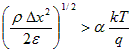 (A.23)
(1)The majority-carrier doping concentration changes too rapidly:
| Dln(Nmaj)| > a(A.24)
(1)The width of the element is too large for its proximity to the surface (This is to ensure an adequate number of small elements near the front or rear surface in case rapidly absorbed light is subsequently applied):
Dx > x. (A.25)
(1)The element consumes too large a fraction of the width of the region:
Dx > wreg/20. (A.26)
(1)The node that would be eliminated by concatenation is the interface between regions or an injection point for the emitter, base, collector, or interface shunt contacts.
The element will be subdivided if either criterion (1) or (4) is true. The number of subelements created will be equal to the ratio of the LHS to the RHS of the equation, with a maximum of 30 subelements permitted.
After a new set of nodes has been selected, the values of the various solution variables at these nodes are obtained by interpolating values from the previous set of nodes. For ND, NA, tno, and tpo, this interpolation assumes that the logarithm of the parameters is linear between nodes; while for y, yeq, fn, fp, A, Vn, Vp, xn, xp, vsat, Et, e, and G it assumes that the values themselves are linear.