The parameters that define a type of material can be stored in binary files having the suffix MAT. Three commands at the bottom of the Material menu allow you to create, retrieve, and store these material files. Several MAT files for the most commonly encountered materials are provided on the distribution diskette with PC1D. Loading a new MAT file will only affect the current region. In addition, the Material menu allows you to examine and modify the following parameters for the current region:
This is the low-frequency (dc) value of the permittivity, expressed as a multiple of the permittivity of free space. This value is also known as the dielectric constant of the material. It defines the amount of charge needed to produce a given electric field in the material.
This command opens a dialog box which contains several parameters that are intrinsic to the band structure of the material.
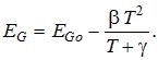
The Band Gap value is used with the Electron Affinity to establish the location of the conduction and valence band edges relative to the vacuum level. For single-region problems they have no effect on the numerical solution, but for heterostructures they affect the discontinuity in the band edges at the interfaces between regions in accordance with an Anderson model of the interface, producing charge dipoles at these locations even if the doping is uniform.
The Nc/Nv Ratio refers to the effective density of states for the conduction and valence bands. This ratio affects the location of the intrinsic energy level within the bandgap, and only affects the solution of heterostructure problems.
Three values can be entered for the intrinsic carrier concentration, at 200, 300 and 400 K. These values are used to interpolate a value for the solution temperature, using a parabolic fit of log(ni) versus 1/T. These values have a major impact on the results obtained for any minority-carrier device.
This dialog box allows you to specify parameters that affect how the recombination rates in this material are influenced by temperature, doping, and electric field. These parameters are often fairly consistent for a given material, and thus are included as material parameters. The base recombination rates for surfaces and bulk are not considered to be a property of the material, and are set separately for each region. See the entry for Region Recombination.
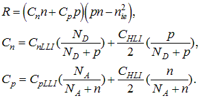
Three Auger recombination coefficients are required to properly compute recombination in either heavily doped or highly injected material. The n-type and p-type coefficients apply to material in low-level injection, while the high-injection coefficient applies to material in high-level injection. The high-injection coefficient represents the sum of both n-type and p-type Auger recombination. It is included as a single factor because in high-level injection the excess electron and hole concentrations are similar. The recombination rate due to Auger processes is computed from the following expression, which weights the result to favor either the low-injection or high-injection coefficients as appropriate:
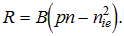
A band-to-band recombination coefficient can be provided. This is primarily important only for direct-bandgap materials. The additional recombination at each point due to coefficient B is given by
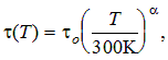
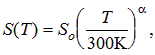
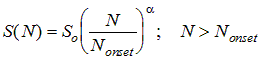
Parameters can be entered for the material to indicate the effect of temperature and doping on SRH surface and bulk recombination. For bulk lifetime, the values of tn and tp specified for the region are modified for use in the SRH recombination formula to reflect the actual device temperature and the local doping density. These parameters can be adjusted to either increase or decrease the impact of temperature and doping. The temperature effect is given by the following formula, applied to both electron and hole lifetimes:
and the doping effect is given by
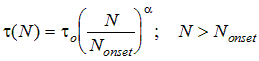
The parameters in these two expressions are empirical and very dependent on the crystal growth technology. For silicon, reasonable choices are -0.5 for the temperature exponent, -0.4 for the doping exponent, and 1E15 cm-3 for the onset.
For surface recombination velocities, both electron and hole values are modified using the following formulas, which have the same form as the bulk-lifetime expressions.
and the surface doping effect is given by
The parameters in these two expressions are very dependent on the surface treatment process. For thermal oxide on n-type silicon, reasonable choices are 0.5 for the temperature exponent, 1.0 for the doping exponent, and 1E18 cm-3 for the onset. No consistent dependence of S on surface doping density has been demonstrated for p-type silicon at the time of this writing.
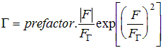
The Hurkx model for trap-assisted tunneling is used. This extends the conventional SRH recombination expression to include trap-assisted tunneling enhanced by the local electric field. This model replaces the carrier lifetimes tn and tp in the SRH model with 
where G is defined by:
 (equation A2 in Hurkx et. al.)
This expression can be parametrised by specifying a prefactor (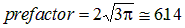 ) and the value of Fgamma at 300K. Hurkx gives:
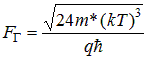 (equation A3 in Hurkx et. al.).
and suggests m*=0.25m0.
WARNING: Do not use this model blindly!
This model is only valid provided the electric field does not get too large. It will be valid in general for midgap traps, but for shallow traps in regions of very high electric field, it may dramatically overestimate the impact of trap-assisted tunneling (for high fields, G no longer depends exponentially on F). In these sitations, the value for the prefactor and for Fgamma can be modified to give more realistic simulations.
At present, there is insufficient experimental data to justify a more complex model, although Hurkx provides an additional high-field equation (eqn A5 of his 1992 paper).
Reference:
G.A.M. Hurkx, D.B.M. Klaassen, and M.P.G. Knuvers, “A New Recombination Model for Device Simulation Including Tunneling”, IEEE Trans. Electron Devices, ED-39, (Feb. 1992), pp. 331-338.
The parameters entered for bandgap narrowing allow the equilibrium pn product to depend on the local doping density according to the following expression:
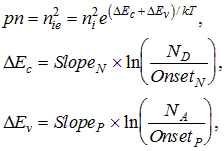
where the log expressions are taken equal to zero for doping densities less than the respective onset values.
The mobilities of electrons and holes can either be set to fixed values throughout the region, or calculated based on the temperature and local doping density using a model. The model uses a different set of coefficients where the carrier is in the minority than where it is in the majority. The expression used has the following form:
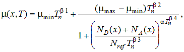
where Tn is the temperature normalized to 300 K. The mobility model also allows for a maximum velocity for each carrier. This is implemented as a reduction in the mobility at each point in the device where the velocity that the carriers would have achieved approaches or exceeds the saturation velocity. The low-field mobility is replaced with a high-field mobility given by:
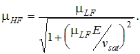
Normally, the electric field is used for “E”. This produces the required mobility reduction in regions where the high carrier velocity is due to a high electric field, as at junctions. A more accurate approach is to use the gradient in the quasi-Fermi potential in place of E in this expression. This can be done in PC1D by selecting Total velocity saturation in the Compute:Numerical dialog box. Note, however, that convergence is less robust and solutions will take much longer with this option selected.
The mobility model does not account for mobility degradation due to carrier-carrier scattering associated with high-level injection.
The index of refraction can be either a fixed value or a function of wavelength using data imported from an external disk file. External index-of-refraction files are standard ASCII files with a filename suffix INR. Each line in the file should contain two numerical values, separated by one or more spaces or a tab. The first value on each line is a value of free-space wavelength, in nm. The second value on each line is the index of refraction at that wavelength. The maximum number of lines allowed is 200. All values of the index must be positive, and the values of wavelength must increase monotonically. If the range of wavelengths provided is less than is required for the solution of a problem, the index of refraction for the first (or last) wavelength is used for all smaller (or larger) wavelengths.
Optical Absorption Coefficients
The optical absorption coefficient as a function of wavelength can be generated as a function of temperature using an internal model, or read from an external disk file. When experimental data for the temperature of interest is available, it is generally better to use this data than to rely on the internal model. Only absorption that leads to photogenerated carriers should be considered, since PC1D assumes that every intinsically absorbed photon produces an electron-hole pair. Parasitic absorption processes can be modelled through the Free-Carrier Absorption dialog.
The internal model for photon absorption includes two direct-gap transitions and eight indirect transitions. The indirect transitions are based on two indirect gaps and either absorption or creation of phonons having two possible energies. Temperature affects the absorption coefficient, a, through a decrease in the energy gaps and through a change in the probability of phonon-assisted transitions. The entries required in the absorption dialog are the energy gaps at 300 K. All four energy gaps are assumed to depend on the absolute temperature (T) through a temperature coefficient (b) and temperature offset (g):
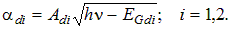
The contributions to the absorption coefficient due to direct transitions for photons with energy hn greater than the energy gap EGdi are given by
The eight phonon-assisted transitions for indirect-gap energies EGi and phonon energies Epj take the form
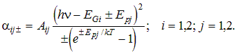
The upper signs correspond to phonon-absorbing transitions, while the lower signs are for phonon-creating transitions. Only those terms for which hn +/- Epj > EGi are included. Otherwise, there is no absorption due to that transition. The indirect-gap absorption is clamped for energies greater than the next-higher direct gap. All ten absorption coefficients are added together to yield the total absorption coefficient for each incident wavelength of light (hn = hc/l, where hc = 1239.8424 eV*nm).
External absorption files are standard ASCII files with a filename suffix ABS. Each line in the file should contain two numerical values, separated by one or more spaces or a tab. The first value on each line is a value of free-space wavelength, in nm. The second value on each line is the absorption coefficient, in cm-1. The maximum number of lines allowed is 200. All values of the absorption coefficient must be positive, and the values of wavelength must increase monotonically. If the range of wavelengths provided is less than is required for the solution of a problem, the absorption coefficient for the first (or last) wavelength is used for all smaller (or larger) wavelengths. For this reason, it is important that the last entry in the file give an absorption coefficient of zero. Otherwise, PC1D will assume that the final (nonzero) value applies even out to very long wavelengths, thereby greatly overestimating the total photogeneration. Room-temperature absorption files are provided with PC1D for several materials.
Free-carrier absorption competes with intrinsic absorption, reducing the fraction of photons which generate electron-hole pairs.
The free-carrier absorption across a device is not only dependent upon the wavelength of incident light, but also depends upon the profile of the carrier concentrations across the device. It can be specified by the free-carrier absorption coefficient, which for monochromatic incident light is assumed to take the form
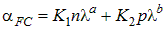
where K1, K2, a, b are empirically determined constants, and l is measured in nm. At the time of writing, estimates of these parameters were available for several materials:
| K1 | a | K2 | b | Source | |
| AlSb | 1.9e-24 | 2 | Fan | ||
| GaAs | 4e-29 | 3 | Fan | ||
| GaP | (1.5e-24) | (1.8) | Fan | ||
| GaSb | 9e-31 | 3.5 | Fan | ||
| Ge | ~5e-25 | ~2 | Fan | ||
| InAs | 6.5e-29 | 3 | Fan | ||
| InP | 5e-27 | 2.5 | Fan | ||
| InSb | 2.8e-25 | 2 | Fan | ||
| Si | 2.6e-27 | 3 | 2.7e-24 | 2 | Schmid |
References:
D.K. Schroder, R.N. Thomas, and J.C. Swartz, “Free Carrier Absorption in Silicon”, IEEE Trans. Electron Devices, ED-25, (Feb. 1978), pp. 254-261.
P.E. Schmid, “Optical Absorption in Heavily Doped Silicon”, Phys. Review B (1981), Vol 23, pp. 5531-5536.
H.Y. Fan, “Semiconductors and Semimetals”, ed. R.K. Williamson and A.C. Beer, Academic Press (1967), Vol 3, p.409.
For reasons of speed, PC1D calculates the photogeneration only once for each solution step, using the values of n and p which were calculated for the previous step. For example, the steady-state photogeneration will be based on the equilibrium concentrations of electrons and holes. Although n and p will vary from their equilibrium values, the perturbation is unlikely to have a significant effect.
For the rare situations where the change in n and p during solution is important, the Compute:Continue menu command can be used at the conclusion of a steady-state problem. This will cause the photogeneration to be recalculated, using the values of n and p obtained from the steady-state solution. The steady state solution will then be resolved using the new photogeneration.